LINEAR Low Noise Regulated Charge Pump Design Specifications and User Guide - 2x2 DFN Package
Summary
An efficient low-noise regulated charge pump voltage doubler series designed for portable electronics requiring stable 3.3V or 5V power. Ideal for designers of USB accessories, LED drivers, and handheld devices powered by single or multi-cell batteries. The manual provides comprehensive technical specifications, covering features like automatic Burst Mode operation, ultra-low quiescent current (<1µA), and high efficiency across varying input voltages (1.8V–5.5V).
Page 1 Text Content
LTC3204-3.3/LTC3204-5/ LTC3204B-3.3/LTC3204B-5 Low Noise Regulated Charge Pump in 2 × 2 DFN
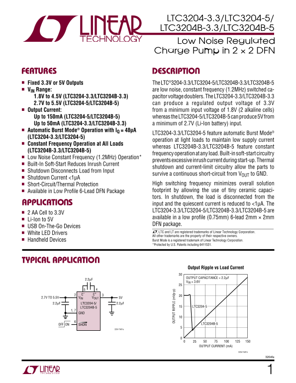
FEATURES DESCRIPTIO ■ Fixed 3.3V or 5V Outputs The LTC®3204-3.3/LTC3204-5/LTC3204B-3.3/LTC3204B-5 ■ VIN Range: are low noise, constant frequency (1.2MHz) switched ca- 1.8V to 4.5V (LTC3204-3.3/LTC3204B-3.3) pacitor voltage doublers. The LTC3204-3.3/LTC3204B-3.3 2.7V to 5.5V (LTC3204-5/LTC3204B-5) can produce a regulated output voltage of 3.3V ■ Output Current: from a minimum input voltage of 1.8V (2 alkaline cells) Up to 150m A (LTC3204-5/LTC3204B-5) whereas the LTC3204-5/LTC3204B-5 can produce 5V from Up to 50m A (LTC3204-3.3/LTC3204B-3.3) a minimum of 2.7V (Li-Ion battery) input. ■ Automatic Burst Mode® Operation with IQ = 48µA
LTC3204-3.3/LTC3204-5 feature automatic Burst Mode®
(LTC3204-3.3/LTC3204-5)
operation at light loads to maintain low supply current
■ Constant Frequency Operation at All Loads
whereas LTC3204B-3.3/LTC3204B-5 feature constant
(LTC3204B-3.3/LTC3204B-5)
frequency operation at any load. Built-in soft-start circuitry
■ Low Noise Constant Frequency (1.2MHz) Operation*
prevents excessive inrush current during start-up. Thermal
■ Built-In Soft-Start Reduces Inrush Current
shutdown and current-limit circuitry allow the parts to
■ Shutdown Disconnects Load from Input
OU TP UT IP PL (m Vp -p survive a continuous short-circuit from VOUT to GND.
■ Shutdown Current <1µA
■ Short-Circuit/Thermal Protection High switching frequency minimizes overall solution ■ Available in Low Profile 6-Lead DFN Package footprint by allowing the use of tiny ceramic capaci-
tors. In shutdown, the load is disconnected from the
APPLICATIO S input and the quiescent current is reduced to <1µA. The
LTC3204-3.3/LTC3204-5/LTC3204B-3.3/LTC3204B-5 are
■ 2 AA Cell to 3.3V
available in a low profile (0.75mm) 6-lead 2mm × 2mm
■ Li-Ion to 5V
DFN package.
■ USB On-The-Go Devices
■ White LED Drivers , LTC and LT are registered trademarks of Linear Technology Corporation. All other trademarks are the property of their respective owners.
■ Handheld Devices Burst Mode is a registered trademark of Linear Technology Corporation.
*Protected by U.S. Patents including 6411531.
TYPICAL APPLICATIO
Output Ripple vs Load Current
OUTPUT CAPACITANCE = 2.2µF
VIN = 3.6V
C– C+ VIN VOUT 5V2.7V TO 5.5V
2.2µF LTC3204-5/ 2.2µF
LTC3204B-5 LTC3204-5
1, 7 GND
OFF ON SHDN LTC3204B-5
3204 TA01a
OUTPUT CURRENT (m A)
3204 TA01b
3204fa
Page Summary Contents For LINEAR Low Noise Regulated Charge Pump Design Specifications and User Guide - 2x2 DFN Package
Manual Details
| Brand | Linear |
|---|---|
| Pages | 12 |
| File Size | 618.41 KB |
| Published | May 29, 2026 |
Enter the captcha to get the download link:

Frequently Asked Questions
What is the minimum input voltage required to operate the LTC3204 devices?
The minimum input voltage varies by model, ranging from 1.8V (for -3.3V versions) to a minimum of 2.7V (for -5V versions).
How does the device manage power consumption during light load conditions?
Models LTC3204-3.3/LTC3204-5 feature automatic Burst Mode operation, maintaining low supply current at light loads.
What level of protection is offered against overcurrent or shorts?
The chip features built-in Soft-Start and Short-Circuit/Thermal Protection, allowing it to survive continuous short-circuits indefinitely.