ST LDLN015xx 150mA Ultra Low Noise High PSRR Linear Voltage Regulator IC Data Manual User Guide
Summary
The LDLN015xx is an ultra low noise linear voltage regulator designed for high-performance and noise-sensitive applications, such as ADCs and VCOs found in mobile phones. Capable of providing a clean 150 mA output current from varying inputs (2.1V–5.5V), it features exceptionally low noise (6.3 µV) and high PSRR. The manual provides comprehensive details on electrical characteristics, pin configuration, maximum ratings, and typical application circuits for seamless integration into sensitive electronic systems.
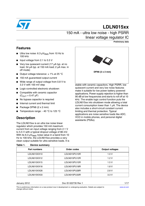
Page 1 Text Content
LDLN015xx
150 m A - ultra low noise - high PSRR
linear voltage regulator IC
Preliminary data
Features Ultra low noise: 6.3 µVRMS from 10 Hz to k Hz Input voltage from 2.1 to 5.5 V Very low quiescent current (17 µA typ. at no load, 54 µA typ. at 150 m A load; 2 µA max. in off mode)
DFN6 (2 x 2 mm)
Output voltage tolerance: ± 1% at 25 °C 150 m A guaranteed output current Wide range of output voltage from 0.8 V to 3.3 V with 100 m V step stable with ceramic capacitors. High PSRR, low
quiescent current and very low noise features
Logic-controlled electronic shutdown
make it suitable for low power battery powered
Compatible with ceramic capacitor
applications. Power supply rejection is higher than
(COUT 0.47 µF)
90 d B at low frequencies and starts to roll off at 10
No bypass capacitor is required k Hz. The enable logic control function puts the
LDLN015xx into shutdown mode allowing a total
Internal current and thermal limit
current consumption lower than 1 µA. The device
Package DFN6 (2 x 2 mm)
also includes a short-circuit constant current
Temperature range: - 40 °C to 125 °C limiting and thermal protection. Typical
applications are noise sensitive loads like ADC, VCO in mobile phones, and personal digital
Description
assistants (PDAs).
The LDLN015xx is an ultra low noise linear regulator which provides 150 m A maximum current from an input voltage ranging from 2.1 V to 5.5 V with a typical dropout voltage of 86 m V. With its 6.3 µVRMS noise value in a band from 10 Hz to 100 k Hz, the LDLN015xx provides a very clean output suitable for ultra sensitive loads. It is Table 1. Device summary
Part numbers Order codes Output voltages
LDLN015XX10 LDLN015PU10R 1.0 V LDLN015XX12 LDLN015PU12R 1.2 V LDLN015XX15 LDLN015PU15R 1.5 V LDLN015XX18 LDLN015PU18R 1.8 V LDLN015XX28 LDLN015PU28R 2.8 V LDLN015XX33 LDLN015PU33R 3.3 V
January 2012 Doc ID 022735 Rev 1 1/17 This is preliminary information on a new product now in development or undergoing evaluation. Details are subject to www.st.com change without notice.
Page Summary Contents For ST LDLN015xx 150mA Ultra Low Noise High PSRR Linear Voltage Regulator IC Data Manual User Guide
Manual Details
| Brand | Linear |
|---|---|
| Pages | 17 |
| File Size | 1.40 MB |
| Published | June 19, 2026 |
Enter the captcha to get the download link:

Frequently Asked Questions
What is the noise performance of this regulator?
It features ultra low noise, measuring 6.3 µV in a band from 10 Hz to RMS 100 kHz.
Is an external bypass capacitor necessary for stable operation?
No bypass capacitor is required; however, it is compatible with ceramic capacitors.
How can I put this device into low-power shutdown mode?
Use the enable logic control function. Applying V < 0.4 V will put the LDLN015xx into shutdown mode.
What is the maximum current output capacity?
The device is guaranteed to provide up to 150 mA of continuous output current.