Texas Instruments TPS799xx 200mA, Low Quiescent Current, Ultra-LOW Noise, High PSRR Low Dropout Linear Regulator Data Sheet User Manual
Summary
This comprehensive manual details the TPS799xx series of Ultra-Low Noise Low Dropout Regulators (LDOs), designed for demanding portable applications. Featuring exceptional performance such as high PSRR, 29.5µV RMS noise, and stable operation from 1.2V to 6.5V at extremely low quiescent currents (40µA). It is the essential component for engineers designing wireless communication systems, including cellular phones, Bluetooth devices, WLAN access points, and sophisticated handheld electronics requiring reliable power management in space-constrained packages.
Page 1 Text Content
查询TPS79901DDC供应商
TPS799xx
www.ti.com
SBVS056G–JANUARY 2005–REVISED AUGUST
200m A, Low Quiescent Current, Ultra-Low Noise, High PSRR
Low Dropout Linear Regulator
FEATURES DESCRIPTION
200m A Low Dropout Regulator with EN
The TPS799xx family of low-dropout (LDO)
Low IQ: 40µA low-power linear regulators offer excellent AC•
performance with very low ground current. High•
Multiple Output Voltage Versions Available:
power-supply rejection ratio (PSRR), low noise, fast
Fixed Outputs of 1.2V to 4.5V Using
start-up, and excellent line and load transient
Innovative Factory EEPROM Programming
response are provided while consuming very low
Adjustable Outputs from 1.20V to 6.5V 40µA (typical) ground current. The TPS799xx is–
stable with ceramic capacitors and uses an•
High PSRR: 66d B at 1k Hz
advanced Bi CMOS fabrication process to yield
Ultra-low Noise: 29.5µVRMS
dropout voltage typically 100m V at 200m A output.
Fast Start-Up Time: 45µs The TPS799xx uses precision voltage reference•
and feedback loop to achieve overall accuracy of 2%•
Stable with Low-ESR, 2.0µF Typical Output
over all load, line, process, and temperature Capacitance
variations. It is fully specified from TJ –40°C to
Excellent Load/Line Transient Response
+125°C and is offered in low profile Thin SOT23,
2% Overall Accuracy (Load/Line/Temp) Wafer Chip-Scale (WCSP), and 2mm 2mm SON•
packages, ideal for wireless handsets and WLAN•
Very Low Dropout: 100m V
cards.
Thin SOT-23, WCSP, and 2mm 2mm SON-6
Packages
APPLICATIONS
Cellular Phones
Wireless LAN, Bluetooth™
VCOs, RF
Handheld Organizers, PDAs
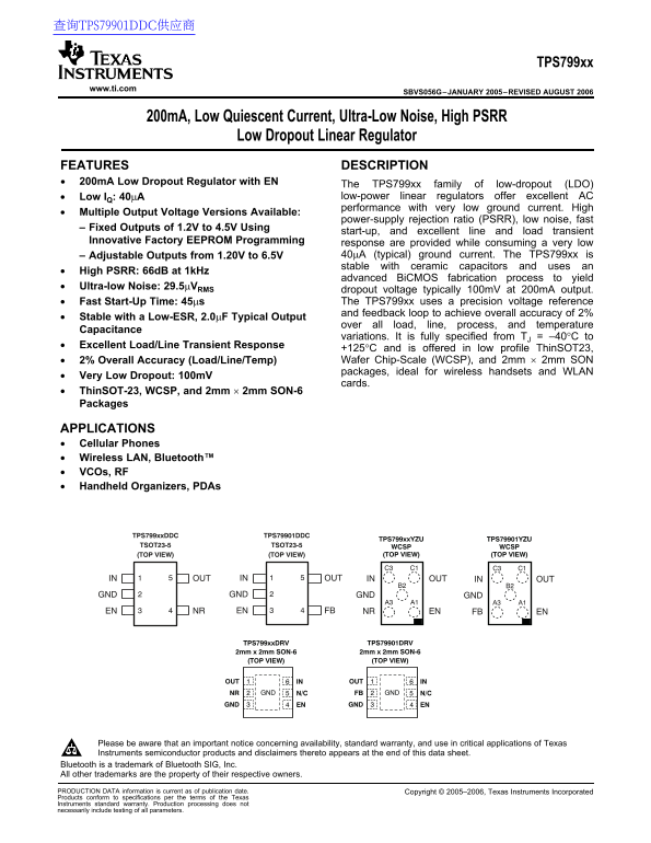
TPS799xx DDC TPS79901DDC
TPS799xx YZU TPS79901YZU
TSOT23-5 TSOT23-5 WCSP WCSP
(TOP VIEW) (TOP VIEW) (TOP VIEW) (TOP VIEW)
IN OUT IN OUT IN OUT IN OUT
GND GND GND GND
EN NR EN FB NR EN FB EN
TPS799xx DRV TPS79901DRV 2mm x 2mm SON-6 2mm x 2mm SON-6 (TOP VIEW) (TOP VIEW)
OUT IN OUT IN
NR GND N/C FB GND N/C
GND EN GND EN
Please be aware that an important notice concerning availability, standard warranty, and use in critical applications of Texas
Instruments semiconductor products and disclaimers thereto appears at the end of this data sheet.
Bluetooth is trademark of Bluetooth SIG, Inc.
All other trademarks are the property of their respective owners.
PRODUCTION DATA information is current as of publication date. Copyright 2005–2006, Texas Instruments Incorporated
Products conform to specifications per the terms of the Texas
Instruments standard warranty. Production processing does not
necessarily include testing of all parameters.
Page Summary Contents For Texas Instruments TPS799xx 200mA, Low Quiescent Current, Ultra-LOW Noise, High PSRR Low Dropout Linear Regulator Data Sheet User Manual
Manual Details
| Brand | Texas Instruments |
|---|---|
| Pages | 21 |
| File Size | 440.51 KB |
| Published | June 01, 2026 |
Enter the captcha to get the download link:

Frequently Asked Questions
What is the typical current consumption of the TPS799xx regulator?
It consumes a very low 40μA (typical) ground current.
How accurate is the voltage regulation?
The overall accuracy for the TPS799xx family is 2% (Load/Line/Temp).
What advanced applications can this LDO regulator power?
It is ideal for wireless handsets, WLAN, Bluetooth®, Cellular Phones, and RF VCOs.
What is the minimum dropout voltage attainable?
The very low dropout voltage is typically 100mV at a 200mA output.
Is this device sensitive to static discharge damage?
Yes, it can be damaged by ESD; handling with appropriate precautions is recommended.