LINEAR LT1002 Dual, Matched Precision Operational Amplifier Data Sheet
Summary
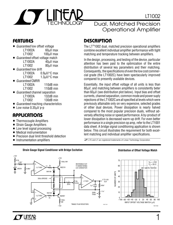
The LT1002 is a high-precision dual operational amplifier designed for demanding scientific and medical instrumentation. It delivers superior performance through extremely low offset voltage, excellent matching between channels, and high common-mode rejection ratio. This manual provides comprehensive electrical specifications, application circuits (including strain gauge conditioning), detailed package information, and technical guidelines for integrating this reliable op-amp into critical sensing applications.
Page 1 Text Content
LT1002
Dual, Matched Precision Operational Amplifier
FEATURES DESCRIPTION
Guaranteed low offset voltage The LT®1002 dual, matched precision operational amplifiers LT1002A 60µV max combine excellent individual amplifier performance with tight LT1002 100µV max matching and temperature tracking between amplifiers. Guaranteed offset voltage match
In the design, processing, and testing of the device, particular
LT1002A 40µV max
attention has been paid to the optimization of the entire
LT1002 80µV max
distribution of several key parameters and their matching.
Guaranteed low drift
Consequently, the specifications of even the low cost commer-
LT1002A 0.9µV/°C max
cial grade (the LT1002C) have been spectacularly improved
LT1002 1.3µV/°C max
compared to presently available devices.
Guaranteed CMRR
LT1002A 110d B min Essentially, the input offset voltage of all units is less than LT1002 110d B min 80µV, and matching between amplifiers is consistently beter Guaranteed channel separation than 60µV (see distribution plot below). Input bias and offset LT1002A 132d B min currents, channel separation, common mode and power suply LT1002 130d B min rejections of the LT1002C are all specified at levels which were Guaranteed maching characteristics previsouly attainable only on very expensive, selected grades Low noise 0.35µV p-p of other dual devices. Power dissipation is nearly halved compared to the most popular precision duals, without ad- APPLICATIONS NU BE OF NI TS versely affecting noise or speed performance. A by-product of lower dissipation is decreased warm-up drift. For even better
Thermocouple Amplifiers
performance in a single precision op amp, refer to the LT1001
Strain Gauge Amplifiers
data sheet. A bridge signal conditioning application is shown
Low level signal processing
below. This circuit illustrates the requirement for both excel-
Medical instrumentation
lent matching and individual amplifier specifications.
Precision dual limit threshold detection
Instrumentation amplifiers , LTC and LT are registered trademarks of Linear Technology Corporation.
Strain Gauge Signal Conditioner with Bridge Excitation Distribution of Offset Voltage Match
100Ω 5W VS = ±15V
REFERENCE OUT TA = 25°C
2k TO MONITORING
1/2LT1002 2N2219
A/D CONVERTER 287 UNITS TESTED
LM329 4.99k*
IN4148
350Ω BRIDGE
0 TO 10V
10k LT1001 OUT*
IN4148 GAIN TRIM
1/2LT1002
5W INPUT OFFSET VOLTAGE MATCH (µV)
*RN60C FILM RESISTORS 1002 TA01
–15V 1002 TA02
Page Summary Contents For LINEAR LT1002 Dual, Matched Precision Operational Amplifier Data Sheet
Manual Details
| Brand | Linear |
|---|---|
| Pages | 16 |
| File Size | 344.74 KB |
| Published | June 05, 2026 |
Enter the captcha to get the download link:

Frequently Asked Questions
What voltage range can I apply differentially to the input?
The differential input voltage is rated up to ±30V.
How well does this amplifier reject noise and common mode signal?
The guaranteed CMRR minimum is 110dB, and the Power Supply Rejection Ratio (PSRR) minimum is 108dB.
What are the operating temperature ranges for different packages?
Ranges vary by package: LT1002AC/LT1002C operates from 0°C to 70°C, while the LT1002AMJ is rated from -55°C to 125°C.
Can this amplifier be used in strain or bridge signal conditioning?
Yes; it is suitable for applications like instrumentation amplifiers, low-level signal processing, and strain gauge/bridge circuit conditioning.