AD826 High-Speed, Low-Power Dual Operational Amplifier Data Sheet Instruction Manual
Summary
This high-speed, low-power dual operational amplifier is designed for power-sensitive applications requiring exceptional stability, such as video processing, active filters, or scanners. The AD826 delivers a robust 50 MHz bandwidth and powerful output drive capability while maintaining the simplicity of single positive voltage supplies (+5V to ±15V). This manual provides comprehensive technical data, including detailed specifications on dynamic performance, input/output characteristics, noise limits, and settling times, ensuring optimal design utilizing its high-speed capabilities in complex analog systems.
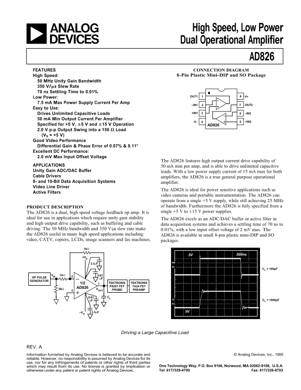
Page 1 Text Content
High Speed, Low Power Dual Operational Amplifier
AD826
FEATURES CONNECTION DIAGRAM
High Speed: 8-Pin Plastic Mini-DIP and SO Package
50 MHz Unity Gain Bandwidth 350 V/ms Slew Rate 70 ns Settling Time to 0.01%
OUT1 V+
Low Power: 7.5 m A Max Power Supply Current Per Amp
–IN1 OUT2
Easy to Use:
Drives Unlimited Capacitive Loads +IN1 –IN2
50 m A Min Output Current Per Amplifier
V– +IN2
Specified for +5 V, 65 V and 615 V Operation AD826 2.0 V p-p Output Swing into a 150 V Load (VS = +5 V) Good Video Performance Differential Gain & Phase Error of 0.07% & 0.118 Excellent DC Performance: 2.0 m V Max Input Offset Voltage
The AD826 features high output current drive capability of
APPLICATIONS m A min per amp, and is able to drive unlimited capacitive Unity Gain ADC/DAC Buffer
loads. With a low power supply current of 15 m A max for both
Cable Drivers
amplifiers, the AD826 is a true general purpose operational
8- and 10-Bit Data Acquisition Systems amplifier. Video Line Driver
The AD826 is ideal for power sensitive applications such as
Active Filters
video cameras and portable instrumentation. The AD826 can operate from a single +5 V supply, while still achieving 25 MHz of bandwidth. Furthermore the AD826 is fully specified from a
PRODUCT DESCRIPTION
single +5 V to ±15 V power supplies.
The AD826 is a dual, high speed voltage feedback op amp. It is ideal for use in applications which require unity gain stability
The AD826 excels as an ADC/DAC buffer or active filter in
and high output drive capability, such as buffering and cable
data acquisition systems and achieves a settling time of 70 ns to
driving. The 50 MHz bandwidth and 350 V/µs slew rate make 0.01%, with a low input offset voltage of 2 m V max. The the AD826 useful in many high speed applications including:
AD826 is available in small 8-pin plastic mini-DIP and SO
video, CATV, copiers, LCDs, image scanners and fax machines.
packages.
5V 500ns
CL = 100p F
1kΩVIN 0.01
HP PULSE µF GENERATOR
1/2 TEKTRONIX TEKTRONIX P6201 FET 7A24 FET
AD826
50Ω VOUT PROBE PREAMP
0.01 CL
µF CL = 1000p F
–VS 3.3µF 5V
Driving a Large Capacitive Load
Information furnished by Analog Devices is believed to be accurate and © Analog Devices, Inc., 1995
reliable. However, no responsibility is assumed by Analog Devices for its use, nor for any infringements of patents or other rights of third parties
which may result from its use. No license is granted by implication or One Technology Way, P.O. Box 9106, Norwood, MA 02062-9106, U.S.A. otherwise under any patent or patent rights of Analog Devices. Tel: 617/329-4700 Fax: 617/326-8703
Page Summary Contents For AD826 High-Speed, Low-Power Dual Operational Amplifier Data Sheet Instruction Manual
Manual Details
| Brand | Dual |
|---|---|
| Pages | 16 |
| File Size | 258.33 KB |
| Published | May 31, 2026 |
Enter the captcha to get the download link:

Frequently Asked Questions
What is the primary function or best application for the AD826 op amp?
It excels as an ADC/DAC buffer, active filter, or video line driver in power-sensitive applications like cameras and portable instrumentation.
What is the maximum operating bandwidth of the device?
The bandwidth can reach up to 50 MHz when supplied with a ±15 V potential difference.
Can this amplifier operate using only a single supply voltage?
Yes, the AD826 can operate from a single +5 V supply while still achieving a 25 MHz bandwidth.
What is the device's capacity for driving capacitive loads?
It has high output current drive capability of 50 mA minimum per amplifier and can drive unlimited capacitive loads.