LINEAR AN75-1 Data Handbook
Summary
This comprehensive technical application note provides detailed schematics and engineering considerations for designing high-performance electronic circuits. It covers topics ranging from low-power voltage-to-frequency conversion to advanced circuit characterization techniques crucial for reliable IC operation. The document assists electrical engineers, embedded systems designers, and researchers in mastering signal conditioning, minimizing parasitic loading, and achieving accurate measurements for complex analog and mixed-signal applications.
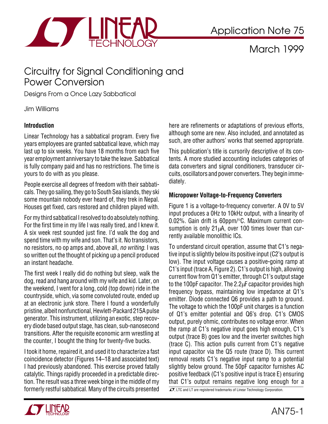
Page 1 Text Content
Application Note 75
March 1999
Circuitry for Signal Conditioning and Power Conversion Designs From a Once Lazy Sabbatical Jim Williams
Introduction here are refinements or adaptations of previous efforts,
although some are new. Also included, and annotated as
Linear Technology has a sabbatical program. Every five
such, are other authors’ works that seemed appropriate.
years employees are granted sabbatical leave, which may last up to six weeks. You have 18 months from each five This publication’s title is cursorily descriptive of its con- year employment anniversary to take the leave. Sabbatical tents. A more studied accounting includes categories of is fully company paid and has no restrictions. The time is data converters and signal conditioners, transducer cir- yours to do with as you please. cuits, oscillators and power converters. They begin imme-
diately.
People exercise all degrees of freedom with their sabbati- cals. They go sailing, they go to South Sea islands, they ski
Micropower Voltage-to-Frequency Converters
some mountain nobody ever heard of, they trek in Nepal.
Houses get fixed, cars restored and children played with. Figure 1 is a voltage-to-frequency converter. A 0V to 5V input produces a 0Hz to 10k Hz output, with a linearity of
For my third sabbatical I resolved to do absolutely nothing.
0.02%. Gain drift is 60ppm/°C. Maximum current con-
For the first time in my life I was really tired, and I knew it.
sumption is only 21µA, over 100 times lower than cur-
A six week rest sounded just fine. I’d walk the dog and
rently available monolithic ICs.
spend time with my wife and son. That’s it. No transistors,
no resistors, no op amps and, above all, no writing. I was To understand circuit operation, assume that C1’s nega- so written out the thought of picking up a pencil produced tive input is slightly below its positive input (C2’s output is an instant headache. low). The input voltage causes a positive-going ramp at C1’s input (trace A, Figure 2). C1’s output is high, allowing
The first week I really did do nothing but sleep, walk the
current flow from Q1’s emitter, through C1’s output stage
dog, read and hang around with my wife and kid. Later, on
to the 100p F capacitor. The 2.2µF capacitor provides high
the weekend, I went for a long, cold (top down) ride in the
frequency bypass, maintaining low impedance at Q1’s
countryside, which, via some convoluted route, ended up
emitter. Diode connected Q6 provides a path to ground.
at an electronic junk store. There I found a wonderfully
The voltage to which the 100p F unit charges is a function
pristine, albeit nonfunctional, Hewlett-Packard 215A pulse
of Q1’s emitter potential and Q6’s drop. C1’s CMOS
generator. This instrument, utilizing an exotic, step recov-
output, purely ohmic, contributes no voltage error. When
ery diode based output stage, has clean, sub-nanosecond
the ramp at C1’s negative input goes high enough, C1’s
transitions. After the requisite economic arm wrestling at
output (trace B) goes low and the inverter switches high
the counter, I bought the thing for twenty-five bucks.
(trace C). This action pulls current from C1’s negative
I took it home, repaired it, and used it to characterize a fast input capacitor via the Q5 route (trace D). This current coincidence detector (Figures 14–18 and associated text) removal resets C1’s negative input ramp to a potential I had previously abandoned. This exercise proved fatally slightly below ground. The 50p F capacitor furnishes AC catalytic. Things rapidly proceeded in a predictable direc- positive feedback (C1’s positive input is trace E) ensuring tion. The result was a three week binge in the middle of my that C1’s output remains negative long enough for a
formerly restful sabbatical. Many of the circuits presented , LTC and LT are registered trademarks of Linear Technology Corporation.
AN75-1
Page Summary Contents For LINEAR AN75-1 Data Handbook
Manual Details
| Brand | Linear |
|---|---|
| Pages | 32 |
| File Size | 495.81 KB |
| Published | July 16, 2026 |
Enter the captcha to get the download link:

Frequently Asked Questions
What is the maximum current consumption for the voltage-to-frequency converter?
The supply current consumption of the v/f converter is only 21μA.
What types of circuits are discussed that utilize signal conditioning and power conversion?
The manual covers data converters, signal conditioners, transducer circuits, oscillators, and power converters.