LINEAR AN39-1 Data Sheet
Summary
Optimize your power supply designs by understanding complex parasitic capacitance effects in step-up transformers. This technical manual provides an in-depth analysis of how circuit components generate resonant spikes, transient voltage swings, and current overloads in high-frequency switching systems. It is essential reading for electrical engineers and power electronics designers tackling demanding high-voltage DC-DC converters needing reliable, optimal performance.
Page 1 Text Content
Application Note 39 February 1990
Parasitic Capacitance Effects in Step-Up Transformer Design Brian Huffman
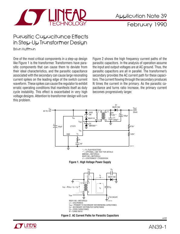
One of the most critical components in a step-up design Figure 2 shows the high frequency current paths of the like Figure 1 is the transformer. Transformers have para- parasitic capacitors. In the analysis of operation assume sitic components that can cause them to deviate from the input and output voltages are at AC ground. Thus, the their ideal characteristics, and the parasitic capacitance parasitic capacitors are all in parallel. The transformer’s associated with the secondary can cause large resonating secondary provides the AC current path for these capaci- current spikes on the leading edge of the switch current tors. The current flowing through the secondary produces waveform. These spikes can cause the regulator to exhibit N times the current in the primary. As the parasitic ca- erratic operating conditions that manifests itself as duty pacitance and turns ratio increase, the primary current cycle instability. This effect is exacerbated in very high becomes progressively larger. voltage designs. Attention to transformer design will cure this problem.
D1 MUR1100
8V TO 15V
VIN C1
MUR110
D2 LT1070 MBR360**
VFB GND VC 1.82k*
AN39 F01
* = 1% FILM RESISTORS ** = OPTIONAL—SEE TEXT FOR DETAILS MBR360 = MOTOROLA MUR1100 = MOTOROLA L1 = COILTRONICS* CTX30203C04
Figure 1. High Voltage Power Supply
CPS CD
MUR1100
IPRI = N(IPS + IS + ID) CS
ISECONDARY
MUR1100 = MOTOROLA AN39 F02
L1 = COILTRONICS CPS = PRIMARY-TO-SECONDARY INTERWINDING CAPACITANCE CS = SECONDARY DISTRIBUTED CAPACITANCE CD = DIODE CAPACITANCE N = TURNS RATIO
Figure 2. AC Current Paths for Parasitic Capacitors
an39f
AN39-1
Page Summary Contents For LINEAR AN39-1 Data Sheet
Manual Details
| Brand | Linear |
|---|---|
| Pages | 4 |
| File Size | 745.91 KB |
| Published | May 30, 2026 |
Enter the captcha to get the download link:

Frequently Asked Questions
What causes current spikes in a step-up transformer design?
These are caused by the parasitic capacitance, which acts with leakage inductance to form a self-resonating circuit.
How does the secondary output diode affect switch transients?
The diode stores charge during its forward cycle. When reverse recovery occurs, this stored charge causes a momentary low impedance and an amplified primary current spike.
What is the function of the blanking time in high voltage converters?
It eliminates large current spikes that could otherwise occur when the switch turns on by preventing premature current paths.