LINEAR AN71-1 Data Sheet
Summary
Optimizing high-performance Analog-to-Digital Converter (ADC) implementation requires careful circuit design. This guide details essential layout techniques for system designers seeking reliable data acquisition by mitigating electrical noise. It provides critical instructions on best practices for grounding—such as maintaining separate analog and digital ground planes—and effective supply bypassing to ensure ADCs operate at peak performance even within complex, high-speed systems.
Page 1 Text Content
Application Note 71
July1997
The Care and Feeding of High Performance ADCs: Get All the Bits You Paid For William C. Rempfer
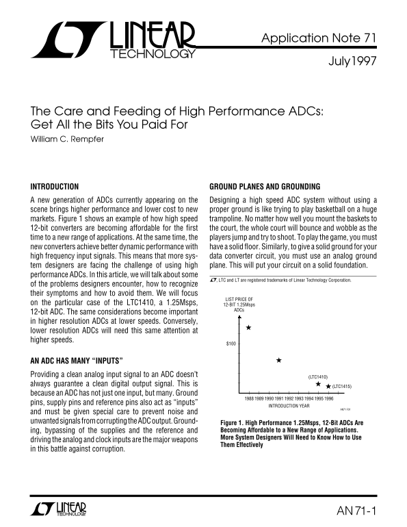
INTRODUCTION GROUND PLANES AND GROUNDING A new generation of ADCs currently appearing on the Designing a high speed ADC system without using a scene brings higher performance and lower cost to new proper ground is like trying to play basketball on a huge markets. Figure 1 shows an example of how high speed trampoline. No matter how well you mount the baskets to 12-bit converters are becoming affordable for the first the court, the whole court will bounce and wobble as the time to a new range of applications. At the same time, the players jump and try to shoot. To play the game, you must new converters achieve better dynamic performance with have a solid floor. Similarly, to give a solid ground for your high frequency input signals. This means that more sys- data converter circuit, you must use an analog ground tem designers are facing the challenge of using high plane. This will put your circuit on a solid foundation. performance ADCs. In this article, we will talk about some
, LTC and LT are registered trademarks of Linear Technology Corporation.
of the problems designers encounter, how to recognize their symptoms and how to avoid them. We will focus
LIST PRICE OF
on the particular case of the LTC1410, a 1.25Msps, 12-BIT 1.25Msps
12-bit ADC. The same considerations become important in higher resolution ADCs at lower speeds. Conversely, lower resolution ADCs will need this same attention at higher speeds.
AN ADC HAS MANY “INPUTS” Providing a clean analog input signal to an ADC doesn’t
(LTC1410)
always guarantee a clean digital output signal. This is
(LTC1415)
because an ADC has not just one input, but many. Ground pins, supply pins and reference pins also act as “inputs”
INTRODUCTION YEAR
AN71 F01
and must be given special care to prevent noise and unwanted signals from corrupting the ADC output. Ground-
Figure 1. High Performance 1.25Msps, 12-Bit ADCs Are ing, bypassing of the supplies and the reference and Becoming Affordable to a New Range of Applications. More System Designers Will Need to Know How to Use
driving the analog and clock inputs are the major weapons
Them Effectively
in this battle against corruption.
AN71-1
Page Summary Contents For LINEAR AN71-1 Data Sheet
Manual Details
| Brand | Linear |
|---|---|
| Pages | 8 |
| File Size | 212.12 KB |
| Published | June 16, 2026 |
Enter the captcha to get the download link:

Frequently Asked Questions
How should analog and digital ground planes be managed?
Use separate analog and digital ground planes, and tie the two grounds together at only one single connection point.
What is required for proper power bypassing on high-speed ADCs?
The key requirement is low lead inductance between the ADC supply pins and the bypass capacitors, positioning caps as close as possible to the supply pins.
Which LTC model offers 12-bit resolution at 1.25Msps?
Both the LTC1410 and LTC1415 models offer 12-bit resolution at a speed of 1.25Msps.