# A B C D E F G H I J K L M N O P Q R S T U V W X Y Z

LINEAR LTC3827-1 Data Sheet

Summary

The LTC3827-1 is a high-performance, dual two-phase synchronous step-down controller designed for advanced power management in battery and distributed DC systems. This comprehensive manual guides engineers through its implementation, detailing features like wide input voltage support (4V–36V), ultra-low quiescent current (80µA), and optimal efficiency across various load conditions. Ideal for designing complex digital devices or industrial electronics requiring stable, dual-rail power output with advanced protection features.
📄 Preview PAGE OF 32

Page 1 Text Content

查询LTC3827-1供应商

POW ER LOSS (m

LTC3827-1

Low IQ, Dual, 2-Phase Synchronous Controller

FEATURES DESCRIPTIO

Wide Output Voltage Range: 0.8V ≤ VOUT ≤ 10V The LTC®3827-1 is a high performance dual step-down Low Operating IQ: 80µA (One Channel On) switching regulator controller that drives all N-channel Out-of-Phase Controllers Reduce Required Input synchronous power MOSFET stages. A constant fre- Capacitance and Power Supply Induced Noise quency current mode architecture allows a phase-lock- OPTI-LOOP® Compensation Minimizes COUT able frequency of up to 650k Hz. Power loss and noise due ±1% Output Voltage Accuracy to the ESR of the input capacitor ESR are minimized by Wide VIN Range: 4V to 36V Operation operating the two controller output stages out of phase.

Phase-Lockable Fixed Frequency 140k Hz to 650k Hz

The 80µA no-load quiescent current extends operating life

Selectable Continuous, Pulse Skipping or Low Ripple

in battery powered systems. OPTI-LOOP compensation

Burst Mode® Operation at Light Loads

allows the transient response to be optimized over a wide

Dual N-Channel MOSFET Synchronous Drive

range of output capacitance and ESR values. The

Very Low Dropout Operation: 99% Duty Cycle LTC3827-1 features a precision 0.8V reference and a Adjustable Output Voltage Soft-Start or Tracking power good output indicator. A wide 4V to 36V input Output Current Foldback Limiting supply range encompasses all battery chemistries. Power Good Output Voltage Monitor

Independent TRACK/SS pins for each controller ramp the

Output Overvoltage Protection

output voltage during startup. Current foldback limits

Low Shutdown IQ: 8µA

MOSFET heat dissipation during short-circuit conditions.

Internal LDO Powers Gate Drive from VIN or VOUT

Small 28-Lead SSOP Package The PLLIN/MODE pin selects among Burst Mode opera-

EF FI CI EN CY

tion, pulse skipping mode, or continuous inductor current

APPLICATIO S mode at light loads. For a leadless package version

(5mm x 5mm QFN) with additional features, see the

Automotive Systems

LTC3827 datasheet.

Battery-Operated Digital Devices

, LTC and LT are registered trademarks of Linear Technology Corporation. Burst Mode

Distributed DC Power Systems and OPTI-LOOP are registered trademarks of Linear Technology Corporation. All other

trademarks are the property of their respective owners. Protected by U.S. Patents, including 5481178, 5929620, 6177787, 6144194, 6100678, 5408150, 6580258, 6304066, 5705919.

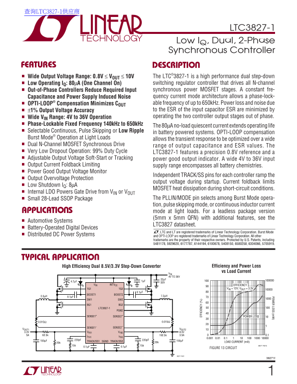
TYPICAL APPLICATIO

High Efficiency Dual 8.5V/3.3V Step-Down Converter Efficiency and Power Loss vs Load Current

VIN 4V TO 36V 22µF

VIN INTVCC EFFICIENCY

TG1 TG2 VIN = 12V; VOUT = 3.3V

BOOST1 BOOST2

SW1 SW2

BG1 BG2

LTC3827-1

SENSE1+ SENSE2+ POWER LOSS

SENSE1– SENSE2–

VOUT1 VOUT2

3.3V VFB1 VFB2 8.5V

ITH1 ITH2

TRACK/SS1 SGND TRACK/SS2 LOAD CURRENT (m A)

15k 15k 38271 TA01b

FIGURE 13 CIRCUIT

38271 TA01

Page Summary Contents For LINEAR LTC3827-1 Data Sheet

Page 1 查询LTC3827-1供应商 POW ER LOSS (m LTC3827-1 Low IQ, Dual, 2-Phase Synchronous Controller FEATURES DESCRIPTIO Wide Output Voltage Range: 0.8V ≤ VOUT ≤ 10V The LTC®3827-1 is a high performance dual step-dow...
Page 2 LTC3827-1 ABSOLUTE AXI U RATI GS PACKAGE/ORDER I FOR ATIO (Note 1) TOP VIEW Input Supply Voltage (VIN) .........................36V to –0.3V ITH1 TRACK/SS1 Top Side Driver Voltages VFB1 PGOOD1 (BOOST1...
Page 3 LTC3827-1 ELECTRICAL CHARACTERISTICS The ● denotes the specifications which apply over the full operating temperature range, otherwise specifications are at TA = 25°C. VIN = 12V, VRUN/SS1, 2 = 5V unle...
Page 4 LTC3827-1 EF FI CI EN CY TYPICAL PERFOR A CE CHARACTERISTICS Efficiency and Power Loss vs Output Current Efficiency vs Load Current Efficiency vs Input Voltage Burst Mode OPERATION VIN = 12V FORCED CO...
Page 5 AX IM UM UR RE NT EN SE OL TA GE (V CU RR EN SE NS TH RE SH OL (m V) SU PP LY UR RE NT (µ A) LTC3827-1 TYPICAL PERFOR A CE CHARACTERISTICS Total Input Supply Current EXTVCC Switchover and INTVCC vs In...
Page 6 IN PU CU RR EN (µ A) IN TV OL TA GE (V TR AC K/ SS UR RE NT (µ A) LTC3827-1 TYPICAL PERFOR A CE CHARACTERISTICS TRACK/SS Pull-Up Current Shutdown (RUN) Threshold Regulated Feedback Voltage vs Temperat...
Page 7 LTC3827-1 PI FU CTIO S ITH1, ITH2 (Pins 1, 13): Error Amplifier Outputs and this voltage source. Must be decoupled to power ground with Switching Regulator Compensation Points. Each associa- a minimum...
Page 8 LTC3827-1 FU CTIO AL DIAGRA PLLIN/MODE INTVCC VIN DUPLICATE FOR SECOND FIN PHASE DET CONTROLLER CHANNEL 100k BOOST PLLLPF TG CB RLP OUT CIND OSCILLATOR 26, 15 CLK2 DET BOT FC CLP 0.88V TOP ON SWITCH I...
Page 9 LTC3827-1 (Refer to Functional Diagram)OPERATIO Main Control Loop close to VOUT, the loop may enter dropout and attempt to turn on the top MOSFET continuously. The dropout detec- The LTC3827-1 uses a ...
Page 10 LTC3827-1 (Refer to Functional Diagram)OPERATIO Light Load Current Operation (Burst Mode Operation, resumes normal operation by turning on the top exter- Pulse Skipping, or Continuous Conduction) nal ...
Page 11 LTC3827-1 (Refer to Functional Diagram)OPERATIO Frequency Selection and Phase-Locked Loop (PLLLPF Output Overvoltage Protection and PLLIN/MODE Pins) An overvoltage comparator guards against transient ...
Page 12 LTC3827-1 (Refer to Functional Diagram)OPERATIO 5V SWITCH 20V/DIV 3.3V SWITCH 20V/DIV INPUT CURRENT 5A/DIV INPUT VOLTAGE 500m V/DIV IN PU RM CU RR EN (A 38271 F01a IIN(MEAS) = 1.55ARMS 38271 F01b IIN(...
Page 13 LTC3827-1 APPLICATIO S I FOR ATIO RSENSE Selection For Output Current of smaller inductor and capacitor values. So why would anyone ever choose to operate at lower frequencies with RSENSE is chosen ba...
Page 14 LTC3827-1 APPLICATIO S I FOR ATIO core material saturates “hard,” which means that induc- The MOSFET power dissipations at maximum output tance collapses abruptly when the peak design current is curre...
Page 15 LTC3827-1 APPLICATIO S I FOR ATIO CIN and COUT Selection The benefit of the LTC3827-1 2-phase operation can be calculated by using the equation above for the higher power The selection of CIN is simpl...
Page 16 LTC3827-1 APPLICATIO S I FOR ATIO Setting Output Voltage The LTC3827-1 output voltages are each set by an external feedback resistor divider carefully placed across the out- put, as shown in Figure 3....
Page 17 LTC3827-1 OU TP UT OL TA GE OU TP UT OL TA GE APPLICATIO S I FOR ATIO VOUTVx Alternatively, the TRACK/SS pin can be used to track two (or more) supplies during start-up, as shown qualitatively RB 1/2 ...
Page 18 LTC3827-1 APPLICATIO S I FOR ATIO INTVCC current is limited to less than 24m A from a 24V sup- 1µF VIN ply when in the G package and not using the EXTVCC supply: TJ = 70°C + (24m A)(24V)(95°C/W) = 125...
Page 19 LTC3827-1 APPLICATIO S I FOR ATIO the input supply: VBOOST = VIN + VINTVCC. The value of the VOUT returns to a safe level, normal operation automati- boost capacitor CB needs to be 100 times that of t...
Page 20 LTC3827-1 FR EQ UE NC (k Hz APPLICATIO S I FOR ATIO Table 2 summarizes the different states in which the PLLLPF pin can be used. Table 2 PLLLPF PIN PLLIN/MODE PIN FREQUENCY 0V DC Voltage 250k Hz Float...
Page 21 LTC3827-1 APPLICATIO S I FOR ATIO Efficiency Considerations tor, and input and output capacitor ESR. In continuous mode the average output current flows through L and The percent efficiency of a switc...
Page 22 LTC3827-1 APPLICATIO S I FOR ATIO Checking Transient Response gain and phase. An output current pulse of 20% to 80% of full-load current having a rise time of 1µs to 10µs will The regulator loop respo...
Page 23 LTC3827-1 APPLICATIO S I FOR ATIO Design Example MOSFET results in: RDS(ON) = 0.035Ω/0.022Ω, CMILLER = 215p F. At maximum input voltage with T(estimated) = 50°C: As a design example for one channel, a...
Page 24 LTC3827-1 APPLICATIO S I FOR ATIO PC Board Layout Checklist 2. Are the signal and power grounds kept separate? The combined IC signal ground pin and the ground return When laying out the printed circu...
Page 25 LTC3827-1 APPLICATIO S I FOR ATIO not be along the high current input feeds from the input 6. Keep the switching nodes (SW1, SW2), top gate nodes capacitor(s). (TG1, TG2), and boost nodes (BOOST1, BOO...
Page 26 LTC3827-1 APPLICATIO S I FOR ATIO PC Board Layout Debugging voltage lockout circuit by further lowering VIN while moni- toring the outputs to verify operation. Start with one controller on at a time. ...
Page 27 EF FI CI EN CY LTC3827-1 TYPICAL APPLICATIO CSS1 0.01µF CITH1A CITH1 RB1 RITH1 ITH1 TRACK/SS1 VFB1 PGOOD1 L1 RSNS1 SENSE1+ TG1 MTOP1 VOUT1 SENSE1– SW1 1n F COUT1 CB1 0.47µF 5A PLLLPF BOOST1 PLLIN/MODE...
Page 28 EF FI CI EN CY LTC3827-1 TYPICAL APPLICATIO High Efficiency Dual 5V/9.5V Step-Down Converter CSS1 0.01µF CITH1A 100P CITH1 RB1 RITH1 ITH1 TRACK/SS1 VFB1 PGOOD1 L1 RSNS1 SENSE1+ TG1 MTOP1 C1 VOUT1 SENS...
Page 29 LTC3827-1 TYPICAL APPLICATIO High Efficiency Synchronizable Dual 5V/8V Step-Down Converter CSS1 0.01µF CITH1A CITH1 RB1 RITH1 ITH1 TRACK/SS1 VFB1 PGOOD1 L1 RSNS1 SENSE1+ TG1 MTOP1 C1 VOUT1 SENSE1– SW1...
Page 30 LTC3827-1 TYPICAL APPLICATIO High Efficiency Dual 1.2V/1V Step-Down Converter CSS1 0.01µF CITH1A CITH1 RB1 RITH1 ITH1 TRACK/SS1 VFB1 PGOOD1 L1 RSNS1 SENSE1+ TG1 MTOP1 C1 VOUT1 SENSE1– SW1 CB1 0.47µF C...
Page 31 LTC3827-1 PACKAGE DESCRIPTIO G Package 28-Lead Plastic SSOP (5.3mm) (Reference LTC DWG # 05-08-1640) 0.42 ±0.03 0.65 BSC RECOMMENDED SOLDER PAD LAYOUT BSC 0.05 NOTE: (.002) 1. CONTROLLING DIMENSION: M...
Page 32 LTC3827-1 TYPICAL APPLICATIO High Efficiency Dual 3.3V/8.0V Step-Down Converter CSS1 0.01µF CITH1A 39p F 100p F CITH1 RITH1 RB1 ITH1 TRACK/SS1 VFB1 PGOOD1 L1 RSNS1 SENSE1+ TG1 MTOP1 C1 VOUT1 SENSE1– S...

Manual Details

Brand Linear
Pages 32
File Size 520.41 KB
Published June 02, 2026
63 views

Enter the captcha to get the download link:

captcha

Frequently Asked Questions

What is the operating temperature range?

The LTC3827-1 operates in a temperature range of –40°C to 85°C.

Does it have low current consumption or complex modes?

It features an ultra-low quiescent current (8µA shutdown, 80µA no-load) and supports Burst Mode, Pulse Skipping, or Continuous operation for efficiency in battery systems.

What voltage range can the input supply handle?

The device accepts a wide input supply voltage ranging from 4V to 36V.

How is output voltage accuracy achieved?

Output voltage accuracy is maintained by operating the two controller output stages out of phase (OPTI-LOOP compensation).