Page 1
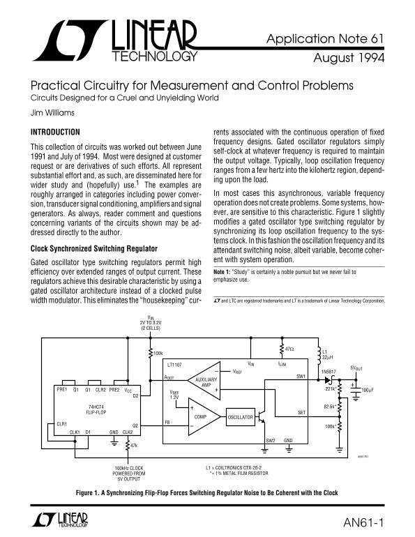
Application Note 61 August 1994 Practical Circuitry for Measurement and Control Problems Circuits Designed for a Cruel and Unyielding World Jim Williams INTRODUCTION rents associated with the continuo...
Page 2
Application Note 61 Circuit operation is best understood by temporarily ignor- The CLR1-CLK1 line monitors output voltage via the ing the flip-flop and assuming the LT1107 regulator’s resistor string....
Page 3
Application Note 61 mechanism. The 1.5V powered LT1073 switching regula- IN IM UM IN PU VO LT AG TO AI NT AI UT VOUT = 5V tor forms a start-up loop. When power is applied the LT1073 runs, causing its ...
Page 4
Application Note 61 L1 AX IM UM OA CU RR EN (m 5VOUT CELL 301k VINILIM VIN SHDN SET SW1 SW FB LT1073 LT1302 NC FB AO ILIM VC GND SW2 PGND GND 4.99k AN61 F06 C1 = AVX TPSD476M016R0150 L1 = COILCRAFT DO...
Page 5
Application Note 61 Low Power, Low Voltage Cold Cathode Fluorescent The Royer converter oscillates at a frequency primarily set Lamp Power Supply by T1’s characteristics (including its load) and the 0...
Page 6
Application Note 61 Circuit efficiency ranges from 80% to 88% at full load, fashion, causing negative biased step-up at T1’s second- depending on line voltage. Current mode operation com- ary. D1 prov...
Page 7
Application Note 61 start-up and sustaining functions have been combined about 3500V to appear at its secondary. The capacitors into a single, closed-loop current source with over 10k V of and diodes ...
Page 8
Application Note 61 in this case 6.5m A. Other currents are obtainable by inverters use a large transformer to generate the 400Hz varying the 190Ω value. The 1N4002 diode string clamps 95V square wave...
Page 9
Application Note 61 3.3V Powered Barometric Pressure Signal A1’s output biases the LT1172 switching regulator’s oper- Conditioner ating point, producing a stepped up DC voltage which appears as T1’s d...
Page 10
Application Note 61 total power consumption to about 1m A. In shutdown the Single Cell Barometers 3.3V powered A/D’s output data remains valid. In practice, It is possible to power these circuits from...
Page 11
Application Note 61 A2 LT1101 OUTPUT 0 TO 3.100V= LT1078 0 TO 31.00"Hg 10k CAL AA CELL A1 1/2 LT1078 ILVIN 1N5818 FB SW1 TRIM FOR 150m V AT 100k LT1110 POINT “A” SET AONC NC SW2GND LT1004-1.2 * =...
Page 12
Application Note 61 NO VA SE NS OR 0V 3. 0V NP H- 8- 0A H† OU TP UT TO 1. "H g. A2 LT NO N- PO LA 1% R2 NI CH IC ON R1 PL FB SW AO SE 0Ω 0. 1% GN SW AA EL LT -1 .2 NO IN AL AL UE . E AC SE NS OR ...
Page 13
Application Note 61 Until recently, this type of accuracy and stability has only The LTC485 RS485 transceiver is set up in the transmit been attainable with bonded strain gauge and capacitively- mode....
Page 14
Application Note 61 LTC1150 OUTPUT LT1097 + INPUT Q1 Q2 OPTIONAL OVER COMPENSATION – INPUT * = 1% FILM RESISTOR R2 Q1, Q2 = 2SK147 TOSHIBA Ω10 AN61 F18 Figure 18. Chopper-Stabilized FET Pair Combines ...
Page 15
Application Note 61 Figure 20 shows the response (trace B) to a 1m V input High Speed Adaptive Trigger Circuit step (trace A). The output is clean, with no overshoots or Line receivers often require a...
Page 16
Application Note 61 Wideband, Thermally-Based RMS/DC Converter loop compensation. The RC network in A1’s output pre- vents it from seeing high speed edges coupled through Applications such as wideband...
Page 17
Application Note 61 ZE RO RI (T RI FU LL -S CA LE LT 1V 1/ LT RM 1k DC Hz A2 0Ω 0Ω LT Q2 SD 0Ω 2N LT 0. LT FU LL -S CA LE 0. 01A1 TR IM Hz UT 0Ω 1/ LT TR IM D1 D2 C1 1/ LT –+ 1/ LT 1% IL ES IS TO 0. O...
Page 18
Application Note 61 ER RO Performance for the circuit is quite impressive. Figure 23 nient current transformers are the “clip-on” type, com- plots error from DC to 11MHz. The graph shows 1% error merc...
Page 19
Application Note 61 DC AND LOW FREQUENCY OUTPUT (TYPICAL) CONCEPTUAL MODEL OF HALL EFFECT SENSOR-XFORMER. TEKTRONIX 120-0464-00 OR 120-0464-02 COMPOSITE OUTPUT TO OPTIONAL ATTENUATOR AND WIDEBAND AMPL...
Page 20
Application Note 61 TO ID EB AN AM PL IF IE SE CT IO Fi gu re re pr od uc ed ith er is si on of ek tro ni x, In c. AN Fi gu re 5. ek tro ni P- al l E ffe ct as ed ur re nt ro be er vo oo p. Fi gu re R...
Page 21
Application Note 61 Triggered 250 Picosecond Rise Time Pulse Generator width modulates at its 100k Hz clock rate. L1’s inductive events are rectified and stored in the 2µF output capacitor. Verifying ...
Page 22
Application Note 61 Some special considerations are required to optimize mandate a separate 12V supply and pulse forming cir- circuit performance. L2’s very small inductance combines cuitry. Figure 29...
Page 23
Application Note 61 3.3VIN f OUT 0k Hz TO A = 5V/DIV 3k Hz LTC1043 B = 5V/DIV 22k LT1034 C = 0.1V/DIV 22µF A, B = 1ms/DIV C = 50µs/DIV AN61 F30 FULL SCALE 3.3VIN Figure 30. Flash Memory Programmer Wav...
Page 24
Application Note 61 stay there. When A1’s output is low the LTC1043’s internal temperature characteristic that opposes C1’s – 120ppm/ oscillator sees C2 and will begin oscillation if A1 remains °C dri...
Page 25
Application Note 61 ductance amplifier. A3’s output feeds LT1228 A4, a cur- rent feedback amplifier. A4’s output, also the circuit’s output, is sampled by the A5-based gain control configu- ration. Th...
Page 26
Application Note 61 Figure 37’s similar circuit substitutes a standard zener for is sampled by the A5-based gain control configuration. the noise source but is more complex and requires a trim. This c...
Page 27
Application Note 61 Switchable Output Crystal Oscillator oscillation commences at the crystals resonant frequency. If D1 and its associated 1k value are realized, oscillation Figure 38’s simple crysta...
Page 28
Application Note 61 7. Williams, J., “High Speed Amplifier Techniques,” Lin- 14. Tektronix, Inc. “P6042 Current Probe Operating and ear Technology Corporation, Application Note 47, Service Manual,” 19...
Page 29
Application Note 61 Copyright 1965 Hewlett-Packard Co. Reproduced with permission. Figure A1. The “Impedance Converter Assembly,” H-P’s Equivalent of Figure 22’s Wideband FET Buffer Note 3: Although J...
Page 30
Application Note 61 Fi gu re 2. he ew le tt- Pa ck ar A’ id eb an In pu t B uf fe r. uv is to r T rio de (U pp er en te r) ro vi de Sp ee d, ow oi se , a nd ig Im pe da nc e. Ci rc ui t R eq ui re V, ...
Page 31
Application Note 61 If that’s not enough to make you propose marriage to Copyright 1965 Hewlett-Packard Co. Reproduced with permission. modern high speed monolithic amplifiers, consider the design her...
Page 32
Application Note 61 Co py rig ht He le tt- Pa ck ar Co Re pr od uc ed ith er is si on Fi gu re 3. -P ’s id eb an Am pl ifi er , t he Vi de Am pl ifi er ss em bl y” on ta in ed an AC ee db ac Lo op s, ...
Page 33
Application Note 61 Fi gu re 4. he ol tm et er “V id eo pl ifi er Re ce iv ed In pu t a t B oa rd ’s ef t S id e. pl ifi er ut pu t D ro ve hr ou de Th er al on ve rte r a t L ow er ig ht . N ot Hi gh...
Page 34
Application Note 61 Copyright 1965 Hewlett-Packard Co. Reproduced with permission. Note 4: In 1965 almost all thermal converters utilized matched pairs of Note 5: The low level chopping technology of ...
Page 35
Application Note 61 Co py rig ht He le tt- Pa ck ar Co Re pr od uc ed ith er is si on Fi gu re 5. -P ’s he rm al on ve rte r ( “A 4” ) a nd on tro l A pl ifi er (“ A6 ”) er fo rm im ila rly to ex t F ...
Page 36
Application Note 61 Fi gu re 6. ho pp er pl ifi er oa rd ee db ac Co nt ro lle th Th er al on ve rte r. ve r F ift Co po ne nt er Re qu ire d, In cl ud in Ne on am ps , P ho to ce lls nd ix ra ns is t...
Page 37
Application Note 61 Fi gu re 7. ig ur ’s irc ui t P ut En tir HP le ct ro ni cs On Sm al l B oa rd . F ET uf fe r- LT pl ifi er pp ea r L ef t C en te Be hi nd NC hi el d. T1 IC (U pp er en te r) ep l...
Page 38
Application Note 61 When casually constructing a wideband amplifier with a few mini-DIPs, the reader will do well to recall the pain and skill expended by the HP3400A’s designers some 30 years ago. In...
Page 39
Application Note 61 Te is the physical temperature that a load (with the same When amplifying noise it is important to remember that impedance as the noise diode) must be at to generate the the noise ...
Page 40
Application Note 61 LT/GP 0894 10K • PRINTED IN USALinear Technology Corporation 1630 Mc Carthy Blvd., Milpitas, CA 95035-7487 AN61-40 (408) 432-1900 ● FAX: (408) 434-0507 ● TELEX: 499-3977 LINEAR T...