# A B C D E F G H I J K L M N O P Q R S T U V W X Y Z

LINEAR AN120-1 Data Sheet

Summary

This technical document serves as an essential resource for designing ultra-precision instrumentation utilizing high-accuracy 18-bit Digital-to-Analog Converters (DACs). It provides comprehensive guidance on critical performance metrics, including precise measurements of Settling Time, Slew Rate, and Ring Time. The manual details component selection and advanced techniques needed to achieve parts-per-million accuracy. It is designed for specialist engineers working in demanding fields such as inertial navigation systems, medical apparatus, and specialized data acquisition requiring extremely low error tolerances.
📄 Preview PAGE OF 36

Page 1 Text Content

Application Note 120

March 2010

1ppm Settling Time Measurement for a Monolithic 18-Bit DAC When Does the Last Angel Stop Dancing on a Speeding Pinhead? Jim Williams Introduction DAC INPUT

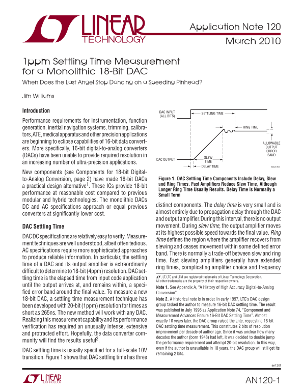
SETTLING TIME

(ALL BITS)

Performance requirements for instrumentation, function

generation, inertial navigation systems, trimming, calibra- RING TIME

tors, ATE, medical apparatus and other precision applications are beginning to eclipse capabilities of 16-bit data convert- ALLOWABLE

OUTPUT

ers. More specifi cally, 16-bit digital-to-analog converters

ERROR (DACs) have been unable to provide required resolution in BAND

DAC OUTPUT

an increasing number of ultra-precision applications.

DELAY TIME AN120 F01

New components (see Components for 18-bit Digital-

to-Analog Conversion, page 2) have made 18-bit DACs Figure 1. DAC Settling Time Components Include Delay, Slew and Ring Times. Fast Amplifi ers Reduce Slew Time, Although

a practical design alternative1. These ICs provide 18-bit

Longer Ring Time Usually Results. Delay Time is Normally a

performance at reasonable cost compared to previous

Small Term

modular and hybrid technologies. The monolithic DACs

distinct components. The delay time is very small and is

DC and AC specifi cations approach or equal previous

almost entirely due to propagation delay through the DAC

converters at signifi cantly lower cost.

and output amplifi er. During this interval, there is no output DAC Settling Time movement. During slew time, the output amplifi er moves at its highest possible speed towards the fi nal value. Ring

DAC DC specifi cations are relatively easy to verify. Measure-

time defi nes the region where the amplifi er recovers from

ment techniques are well understood, albeit often tedious.

slewing and ceases movement within some defi ned error

AC specifi cations require more sophisticated approaches

band. There is normally a trade-off between slew and ring

to produce reliable information. In particular, the settling

time. Fast slewing amplifi ers generally have extended

time of a DAC and its output amplifi er is extraordinarily

ring times, complicating amplifi er choice and frequency

diffi cult to determine to 18-bit (4ppm) resolution. DAC set-

L, LT, LTC and LTM are registered trademarks of Linear Technology Corporation.

tling time is the elapsed time from input code application

All other trademarks are the property of their respective owners.

until the output arrives at, and remains within, a speci-

Note 1. See Appendix A, “A History of High Accuracy Digital-to-Analog

fi ed error band around the fi nal value. To measure a new Conversion”.

18-bit DAC, a settling time measurement technique has Note 2. A historical note is in order. In early 1997, LTC’s DAC design group tasked the author to measure 16-bit DAC settling time. The result

been developed with 20-bit (1ppm) resolution for times as

was published in July 1998 as Application Note 74, “Component and

short as 265ns. The new method will work with any DAC.

Measurement Advances Ensure 16-Bit DAC Settling Time”. Almost

Realizing this measurement capability and its performance exactly 10 years later, the DAC group raised the ante, requesting 18-bit

verifi cation has required an unusually intense, extensive DAC settling time measurement. This constitutes 2 bits of resolution improvement per decade of author age. Since it was unclear how many

and protracted effort. Hopefully, the data converter com-

decades the author (born 1948) had left, it was decided to double jump

munity will fi nd the results useful2.

the performance requirement and attempt 20-bit resolution. In this way, even if the author is unavailable in 10 years, the DAC group will still get its

DAC settling time is usually specifi ed for a full-scale 10V

remaining 2 bits.

transition. Figure 1 shows that DAC settling time has three

an120f

AN120-1

Page Summary Contents For LINEAR AN120-1 Data Sheet

Page 1 Application Note 120 March 2010 1ppm Settling Time Measurement for a Monolithic 18-Bit DAC When Does the Last Angel Stop Dancing on a Speeding Pinhead? Jim Williams Introduction DAC INPUT SETTLING TIM...
Page 2 Application Note 120 COMPONENTS FOR 18-BIT D/A CONVERSION Components suitable for 18-bit D/A conversion are temperature. Gain drift is typically 0.25ppm/°C or about members of an elite class. 18 binar...
Page 3 Application Note 120 INPUT STEP TO OSCILLOSCOPE 0V TO 10V DIGITAL TRANSITION INPUT REF SETTLE OUTPUT TO NODE OSCILLOSCOPE –10VREF AN120 F02 Figure 2. Popular Summing Scheme for DAC Settling Time Measu...
Page 4 Application Note 120 INPUT STEP TO OSCILLOSCOPE 0V TO 10V DIGITAL TRANSITION INPUT SWITCH SETTLE OUTPUT TO NODE OSCILLOSCOPE RESIDUE –10VREF AMPLIFIER DELAYED AN120 F03 PULSE GENERATOR Figure 3. Conce...
Page 5 Application Note 120 rate is within the circuits’ bandpass. The circuit’s wide collapse on the falling edge ensures low feedthrough for bandwidth means the switch command transition is under that cond...
Page 6 Application Note 120 SIGNAL SWITCH INPUT CONTROL 0m V TO ±30m V INPUT 10k**7.5k* OUTPUT 0V 0m V TO ±60m V Q1 1/2 LT1228 (0m V TO ±30m V) 50Ω WHEN DRIVING SAMPLE 1/2 LT1228– 3.57k* 15V ISET ABERRATIONS...
Page 7 Application Note 120 increases to approximately 20m V, although settling time to 1m V remains at 40ns. Figure 11, using double expo- sure technique, compares signal channel rise times for CABERRATION ...
Page 8 Application Note 120 TIME CORRECTED SETTLE NODE-RESIDUE AMPLIFIER-SAMPLE INPUT STEP TO GATE DELAY COMPENSATION OSCILLOSCOPE 0V TO 10V NON-SATURATING DIGITAL TRANSITION SAMPLE DAC RESIDUE INPUT GATE AM...
Page 9 Application Note 120 LT1021 10V reference via the precision 10k summing adjustment, corrected in Figure 16, results in a continuous resistors. The LT1021 also furnishes the DAC reference, baseline. Sa...
Page 10 Application Note 120 settling in 50ns. Figure 18 shows post trim response to sample command turn-on. Delay increases to 70ns but aberrations peak only 50μV, settling in 50ns. Figure 19 SAMPLE COMMAND ...
Page 11 Application Note 120 Figure 24 uses noise averaging techniques to measure underdamped and optimum responses, respectively. settling time to 20 bits (1ppm-10μV) without the band Averaging eliminates no...
Page 12 Application Note 120 REFERENCES 16. Korn, G.A. and Korn, T.M., “Electronic Analog and Hybrid Computers,” “Diode Switches,” pg. 223-226. 1. Williams, Jim, “Component and Measurement Advances Mc Graw-Hi...
Page 13 Application Note 120 APPENDIX A A HISTORY OF HIGH ACCURACY DIGITAL-TO-ANALOG CONVERSION People have been converting digital-to-analog quantities navigation system, circa 1962). The fi rst electronical...
Page 14 Application Note 120 APPENDIX B The digital sampling oscilloscope (Figure B1B) eliminates the vertical output amplifi er, but has an attenuator buffer and amplifi ers ahead of the A/D converter. Becau...
Page 15 Application Note 120 INPUT ATTENUATOR ATTENUATOR BUFFER V+ TRIGGER TO HORIZONTAL/ CIRCUITRY SWEEP SECTION ANALOG OSCILLOSCOPE DELAY LINE TO CRT VERTICAL CHANNEL VERTICAL VERTICAL PREAMP OUTPUT INPUT A...
Page 16 Application Note 120 The waveform to be expanded is placed on the screen at less broad than in Figure B4. Additionally, the peak’s posi- a vertical sensitivity that eliminates all off-screen activity....
Page 17 Application Note 120 APPENDIX C pulse-generator input at 200μV/DIV (note 10k-1Ω divider feeding the settle node). Trace B shows the circuit output at A4, delayed by about 44ns. This delay is a small e...
Page 18 Application Note 120 Circuit Trimming Procedure 10. Turn off input pulses. Disconnect the pulse generator and its 50Ω termination. Apply 5V DC to the pulse The following procedure, given in numerical ...
Page 19 Application Note 120 readily adjustable. Because slew time is usually the domi- Best settling results when the compensation capacitor nant lag, it is tempting to select the fastest slewing amplifi er ...
Page 20 Application Note 120 When feedback capacitors are individually trimmed for determine the optimum value by individual trimming optimal response, DAC, amplifi er and compensation ca- with the production...
Page 21 Application Note 120 vertical division region) but generates a huge error 200μs later when its internal clock applies an offset correction. A = 5V/DIV Successive clock cycles progressively chop the er...
Page 22 Application Note 120 A = 10V/DIV B = 10V/DIV C = 10V/DIV D = 10V/DIV E = 10V/DIV AN120 FF02 20μs/DIV (UNCALIBRATED) Figure F2. Serial Interface Operation Includes Input Start Pulse (Trace A), CS/LD (T...
Page 23 Application Note 120 // Okay, now we’re all synchronized. // Since program does not have direct access to the CS/LD line, you // have to rely on the externally applied pulse. while(!input(CONTROL)){} ...
Page 24 Application Note 120 APPENDIX G generator. The coaxial terminator’s construction ensures this substantial current does this, instead of being dumped into the signal ground plane (100m A termination cu...
Page 25 Application Note 120 Connections coaxially mounting probe tip adapters7. Figures G1 to G5 restate the above sermon in visual form while annotating All signal connections to the breadboard must be coax...
Page 26 Application Note 120 AN120 FG02 Figure G2. DAC-Amplifi er Detail. DAC and Output Amplifi er are at Photo Center Left. Precision Summing Resistors (Box-Shaped, Just Below Large Round Capacitor Near Pho...
Page 27 Application Note 120 AN120 FG03 Figure G3. LT1228 Sampling “Switch” (Photo Center) Is Mounted Upside Down, Permitting V– Referred Die Backside To Shield Residual Radiative Coupling, Reducing Sampling ...
Page 28 Application Note 120 AN120 FG04 Figure G4. A Dedicated, Serially Interfaced Settling Time Breadboard. Serial Interface Digital Board is Obscured Beneath Visible Analog Board (See Appendix H, Figure H7...
Page 29 Application Note 120 AN120 FG05 Figure G5. Serially Interfaced Settling Time Breadboard Signal Path Detail. DAC Board is at Left. Precision Resistors Feed Summing Node and Non-Saturating Amplifi er (P...
Page 30 Application Note 120 APPENDIX H HOW DO YOU KNOW IT WORKS? Settling Time Circuit Performance Verifi cation 1V/DIV High Purity Pulse Generator Any prudent investigation requires performance verifi ca- t...
Page 31 Application Note 120 switched by the relay into a 50Ω termination, resulting text to measure type 109 fall-time purity to microvolts3. in a 250ps risetime pulse. Here, charge lines are not The 109 out...
Page 32 Application Note 120 produced these results. The type 109 drives 20 centimeters type 109 (photo left) delivers its pulse via a General Radio 20 of 50Ω GR-874 airline into a high quality GR-874 50Ω cen...
Page 33 Application Note 120 “Pretty Good” Mercury Wetted Reed Relay Pulse Circuit calibration involves adjusting “resonance set” until Generator the relay emits a reasonably pure audible tone. Next, set the ...
Page 34 Application Note 120 APPENDIX I Figure I2, an auto-zero circuit, locks the sample interval zero value to the non-sampled region baseline. It elimi- Auxiliary Circuits nates the need for periodic readj...
Page 35 Application Note 120 for slight errors and should not require readjustment Figure I4 is a simple time calibrator used to verify oscil- once set to equalize the sample interval zero value and the losco...
Page 36 Application Note 120 INPUT PULSE 5V/DIV DAC OUTPUT 25μV/DIV ON 10V STEP (AVERAGED) AN120 BC 2μs/DIV “A part-per-million is a part-per-million. It’s magic. It’s the brass ring. It’s the holy grail of e...

Manual Details

Brand Linear
Pages 36
File Size 2.04 MB
Published June 03, 2026
69 views

Enter the captcha to get the download link:

captcha

Frequently Asked Questions

What exactly constitutes 'settling time' when using a DAC?

It is the elapsed time from input code application until the output voltage arrives at, and remains within, a specified error band around the final value.

Is there a trade-off when selecting components for high-resolution conversion?

Yes, there is normally a trade-off between slew rate/time and ring time needed to produce reliable settling information.

What DACs or amplifiers are recommended for 18-bit D/A conversion?

Suitable components include the LTC2757 DAC, along with amplifiers listed such as LT1001 or LT1012.