IXYS IXDN404/IXDI404/IXDF404 4Ampere Dual Low-Side Ultrafast MOSFET Drivers Owner's Manual - Specifications/User Guide
Summary
This advanced gate driver IC is designed for professional power electronics applications, providing ultrafast control for MOSFETs and IGBTs up to a 4A peak current. The comprehensive manual serves as an essential resource for electrical engineers, detailing performance specifications, thermal management guidelines, optimal PCB layout techniques (including bypassing), and package options. It is specifically suited for designers building Motor Controllers, Switch Mode Power Supplies (SMPS), DC-DC converters, and Class D amplifiers requiring reliable, high-speed switching solutions.
Page 1 Text Content
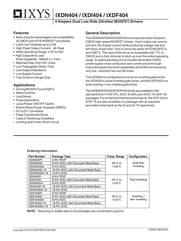
IXDN404 / IXDI404 / IXDF404 4 Ampere Dual Low-Side Ultrafast MOSFET Drivers
Features General Description Built using the advantages and compatibility The IXDN404/IXDI404/IXDF404 is comprised of two 4 Ampere of CMOS and IXYS HDMOSTM processes CMOS high speed MOSFET drivers. Each output can source Latch-Up Protected up to 0.5A and sink 4A of peak current while producing voltage rise and High Peak Output Current: 4A Peak fall times of less than 15ns to drive the latest IXYS MOSFETs Wide Operating Range: 4.5V to 35V and IGBT's. The input of the driver is compatible with TTL or • High Capacitive Load CMOS and is fully immune to latch up over the entire operating Drive Capability: 1800p F in <15ns range. A patent-pending circuit virtually eliminates CMOS • Matched Rise And Fall Times power supply cross conduction and current shoot-through. • Low Propagation Delay Time Improved speed and drive capabilities are further enhanced by Low Output Impedance very low, matched rise and fall times. Low Supply Current
Two Drivers in Single Chip The IXDN404 is configured as a dual non-inverting gate driver, the IXDI404 is a dual inverting gate driver, and the IXDF404 is a Applications dual inverting + non-inverting gate driver.
Driving MOSFETs and IGBTs
The IXDN404/IXDI404/IXDF404 family are available in the
Motor Controls
standard 8 pin P-DIP (PI), SOIC-8 (SIA) and SOIC-16 (SIA-16)
Line Drivers
packages. For enhanced thermal performance, the SOP-8 and
Pulse Generators
SOP-16 are also available in a package with an exposed
Local Power ON/OFF Switch
grounded metal back as the SI and SI-16 repectively.
Switch Mode Power Supplies (SMPS) DC to DC Converters Pulse Transformer Driver Class D Switching Amplifiers Limiting di/dt Under Short Circuit
Ordering Information Part Number Package Type Temp. Range Configuration IXDN404PI 8-Pin PDIP
IXDN404SI 8-Pin SOIC with Grounded Metal Back -55°C to Dual Non IXDN404SIA 8-Pin SOIC +125°C Inverting
IXDN404SI-16 16-Pin SOIC with Grounded Metal Back IXDN404SIA-16 16-Pin SOIC IXDI404PI 8-Pin PDIP
IXDI404SI 8-Pin SOIC with Grounded Metal Back -55°C to Dual Inverting
IXDI404SIA 8-Pin SOIC +125°C IXDI404SI-16 16-Pin SOIC with Grounded Metal Back IXDI404SIA-16 16-Pin SOIC IXDF404PI 8-Pin PDIP
IXDF404SI 8-Pin SOIC with Grounded Metal Back -55°C to Inverting + IXDF404SIA 8-Pin SOIC +125°C Non Inverting
IXDF404SI-16 16-Pin SOIC with Grounded Metal Back IXDF404SIA-16 16-Pin SOIC NOTE: Mounting or solder tabs on all packages are connected to ground
Copyright © IXYS CORPORATION 2004 DS99018B(08/04)
First Release
Page Summary Contents For IXYS IXDN404/IXDI404/IXDF404 4Ampere Dual Low-Side Ultrafast MOSFET Drivers Owner's Manual - Specifications/User Guide
Manual Details
| Brand | Dual |
|---|---|
| Pages | 11 |
| File Size | 760.37 KB |
| Published | May 20, 2026 |
Enter the captcha to get the download link:

Frequently Asked Questions
What functional difference exists between the IXDN404 and IXDI404 models?
The IXDN404 is a dual non-inverting gate driver, while the IXDI404 functions as a dual inverting gate driver.
What are the operating limitations for PCB mounting or heat sinking?
For enhanced thermal performance, SOP-8 and SOP-16 packages can be used with exposed grounded metal back SI/SI-16 versions.
How should I design the power supply bypassing to reduce high-frequency issues?
Keep the output leads as short and wide as possible, and use two different types of low inductance capacitors placed close to the driver itself.
What is the permissible operating temperature range for these drivers?
The device generally supports an operating temperature range from -55°C to 125°C, depending on the specific package type.