ON MC34152, MC33152, NCV33152 High-Speed Dual MOSFET Drivers Data Manual
Summary
These high-speed dual noninverting drivers are purpose-built to interface low-current digital logic signals with demanding power loads. They feature superior performance for driving large capacitive loads, supporting applications in switching power supplies, motor controllers, and DC-to-DC converters. The technical manual provides comprehensive coverage of electrical characteristics, including detailed input/output specifications, package options (SOIC, PDIP), maximum ratings, and specialized suffixes—including automotive versions—making it a vital resource for power electronics design engineers.
Page 1 Text Content
查询MC33152DR2供应商
MC34152, MC33152, NCV33152
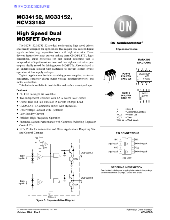
High Speed Dual MOSFET Drivers The MC34152/MC33152 are dual noninverting high speed drivers specifically designed for applications that require low current digital http://onsemi.com signals to drive large capacitive loads with high slew rates. These devices feature low input current making them CMOS/LSTTL logic compatible, input hysteresis for fast output switching that is
MARKING
independent of input transition time, and two high current totem pole DIAGRAMS outputs ideally suited for driving power MOSFETs. Also included is an undervoltage lockout with hysteresis to prevent system erratic operation at low supply voltages.
PDIP−8 MC3x152P
Typical applications include switching power supplies, dc−to−dc
P SUFFIX AWL
converters, capacitor charge pump voltage doublers/inverters, and CASE 626 YYWW
motor controllers. This device is available in dual−in−line and surface mount packages. Features
SOIC−8 3x152
Pb−Free Packages are Available
D SUFFIX
Two Independent Channels with 1.5 A Totem Pole Outputs CASE 7511 Output Rise and Fall Times of 15 ns with 1000 p F Load CMOS/LSTTL Compatible Inputs with Hysteresis
= 3 or 4
Undervoltage Lockout with Hysteresis
= Assembly Location
Low Standby Current
WL, L = Wafer Lot Efficient High Frequency Operation YY, Y = Year WW, W = Work Week
Enhanced System Performance with Common Switching Regulator Control ICs NCV Prefix for Automotive and Other Applications Requiring Site and Control Changes PIN CONNECTIONS
N.C.N.C. Drive Output ALogic Input A VCCGND
Drive Output BLogic Input B
Drive Output A
Logic
Input A (Top View)
ORDERING INFORMATION See detailed ordering and shipping information in the package
dimensions section on page 2 of this data sheet.
Drive Output B
Logic Input B
Figure 1. Representative Diagram
Semiconductor Components Industries, LLC, 2004 Publication Order Number: October, 2004 − Rev. 7 MC34152/D
Page Summary Contents For ON MC34152, MC33152, NCV33152 High-Speed Dual MOSFET Drivers Data Manual
Manual Details
| Brand | Dual |
|---|---|
| Pages | 12 |
| File Size | 152.59 KB |
| Published | May 28, 2026 |
Enter the captcha to get the download link:
