ZETEX ZXMD63P03X Dual 30V P-Channel Enhancement Mode MOSFET Data Manual
Summary
Engineered for high efficiency, this advanced MOSFET device excels in low voltage power management applications due to its combination of low on-resistance and rapid switching speed. The supporting documentation provides comprehensive technical data for designers, detailing absolute maximum ratings, electrical characteristics (including $R_{\text{DS(on)}}$), dynamic switching profiles, thermal performance curves, and package dimensions. It is the optimal component choice for building robust DC-DC converters, motor control systems, and high-performance disconnect switches.
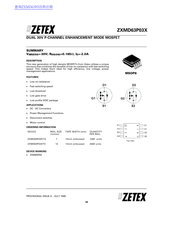
Page 1 Text Content
查询ZXMD63P03X供应商
ZXMD63P03X
DUAL 30V P-CHANNEL ENHANCEMENT MODE MOSFET
SUMMARY V(BR)DSS=-30V; RDS(ON)=0.185V; ID=-2.0A
DESCRIPTION This new generation of high density MOSFETs from Zetex utilises a unique structure that combines the benefits of low on-resistance with fast switching speed. This makes them ideal for high efficiency, low voltage, power management applications.
MSOP8
FEATURES
Low on-resistance
Fast switching speed
Low threshold
Low gate drive
Low profile SOIC package
APPLICATIONS DC - DC Converters
Power Management Functions
Disconnect switches
Motor control
ORDERING INFORMATION
DEVICE REEL SIZE TAPE WIDTH (mm) QUANTITY
(inches) PER REEL
ZXMD63P03XTA 12mm embossed 1000 units
Top View
ZXMD63P03XTC 12mm embossed 4000 units
DEVICE MARKING ZXM63P03
PROVISIONAL ISSUE A - JULY 1999
Page Summary Contents For ZETEX ZXMD63P03X Dual 30V P-Channel Enhancement Mode MOSFET Data Manual
Manual Details
| Brand | Dual |
|---|---|
| Pages | 7 |
| File Size | 211.31 KB |
| Published | June 06, 2026 |
Enter the captcha to get the download link:

Frequently Asked Questions
What material types are best suited for this MOSFET?
These high-density MOSFETs are ideal for low voltage, power management applications such as DC-DC Converters and Motor control.
What is the nominal on-state resistance (Rds(on))?
The static drain-source on-state resistance is 0.185 Ω operating at V = -10V, I = -1.2A.
What are the maximum voltage and temperature limits?
The absolute maximum ratings include a Drain-Source Voltage (VDS) limit of -30V and an operating range from -55 to +150 °C.
How do I determine the power dissipation rating?
It depends on packaging; for surface mounting on 25mm x 25mm FR4 PCB, the recommended power dissipation is 1.25 W.
What services can this MOSFET be used for?
Applications include DC-DC Converters, Power Management Functions, Disconnect switches, and Motor control.