Fairchild NDH834P P-Channel Enhancement Mode Field Effect Transistor Data Handbook
Summary
This detailed technical manual for the NDH834P Power FET provides comprehensive specifications, covering everything from absolute maximum ratings and thermal performance to dynamic on-resistance and switching characteristics. Built using advanced SuperSOT-8 DMOS technology, this transistor features ultra-low R_DS(ON) optimized for reliable, high-speed power delivery. Ideal for electrical engineers developing critical low voltage, battery-powered circuits or portable electronic systems that demand superior thermal management and maximum efficiency.
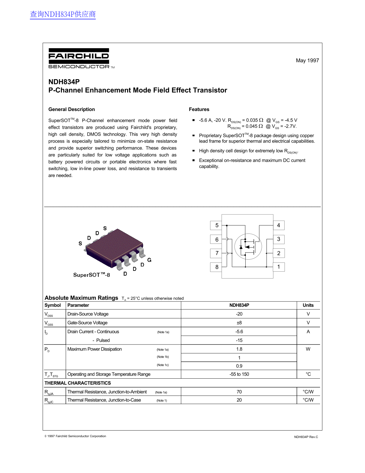
Page 1 Text Content
查询NDH834P供应商
May 1997
NDH834P P-Channel Enhancement Mode Field Effect Transistor
General Description Features
Super SOTTM-8 P-Channel enhancement mode power field -5.6 A, -20 V. RDS(ON) = 0.035 Ω @ VGS = -4.5 V effect transistors are produced using Fairchild's proprietary, RDS(ON) = 0.045 Ω @ VGS = -2.7V.
high cell density, DMOS technology. This very high density
Proprietary Super SOTTM-8 package design using copper process is especially tailored to minimize on-state resistance lead frame for superior thermal and electrical capabilities.
and provide superior switching performance. These devices
High density cell design for extremely low RDS(ON).
are particularly suited for low voltage applications such as
Exceptional on-resistance and maximum DC current
battery powered circuits or portable electronics where fast
capability.
switching, low in-line power loss, and resistance to transients are needed.
Absolute Maximum Ratings TA = 25°C unless otherwise noted Symbol Parameter NDH834P Units VDSS Drain-Source Voltage -20
VGSS Gate-Source Voltage ±8
ID Drain Current - Continuous (Note 1a) -5.6
- Pulsed -15
PD Maximum Power Dissipation (Note 1a) 1.8 (Note 1b)
(Note 1c)
TJ,TSTG Operating and Storage Temperature Range -55 to 150 °C
THERMAL CHARACTERISTICS
Rq JA Thermal Resistance, Junction-to-Ambient (Note 1a) °C/W Rq JC Thermal Resistance, Junction-to-Case (Note 1) °C/W
© 1997 Fairchild Semiconductor Corporation NDH834P Rev.C
Page Summary Contents For Fairchild NDH834P P-Channel Enhancement Mode Field Effect Transistor Data Handbook
Manual Details
| Brand | Fairchild |
|---|---|
| Pages | 8 |
| File Size | 81.39 KB |
| Published | July 07, 2026 |
Enter the captcha to get the download link:

Frequently Asked Questions
What is the maximum voltage for Drain-Source Voltage?
The absolute maximum rating for Drain-Source Voltage (VDS) is -20 V.
Where must thermal resistance calculations take into account user board design?
Thermal characterization and various R values are determined by the user's specific circuit board design, not just by guaranteed qJA/qJC ratings.
What are the recommended applications for this FET?
It is suited for low-voltage applications like battery-powered circuits or portable electronics needing fast switching and low power loss.
How does the package minimize on-state resistance?
The SuperSOT-8 package design, utilizing a copper process, is specifically tailored to minimize on-state resistance for better thermal and electrical performance.