HITACHI 2SK1167, 2SK1168 Silicon N-Channel MOS FET Data Manual
Summary
Discover the 2SK1167 and 2SK1168 N-Channel MOS FETs, essential components engineered for high-speed power switching. These robust devices feature low on-resistance and are ideally suited for demanding power applications such as DC-DC converters and switching regulators. This comprehensive technical manual provides engineers with complete details, including absolute maximum ratings, detailed electrical characteristics, dynamic switching time analysis, and thermal performance curves necessary for reliable circuit design. It is the definitive resource for professionals designing high-efficiency power electronics systems.
Page 1 Text Content
查询2SK1167供应商
2SK1167, 2SK1168 Silicon N-Channel MOS FET
Application
High speed power switching
Features
• Low on-resistance • High speed switching • Low drive current • No secondary breakdown • Suitable for switching regulator and DC-DC converter
Outline
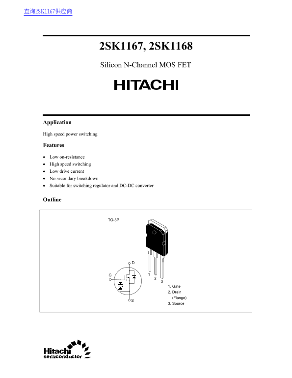
TO-3P
1. Gate 2. Drain (Flange) 3. Source
Page Summary Contents For HITACHI 2SK1167, 2SK1168 Silicon N-Channel MOS FET Data Manual
Manual Details
| Brand | Hitachi |
|---|---|
| Pages | 9 |
| File Size | 45.50 KB |
| Published | June 03, 2026 |
Enter the captcha to get the download link:

Frequently Asked Questions
What applications are these FETs suitable for?
They are suitable for switching regulators and DC-DC converters due to their low on-resistance and high speed switching capability.
What is the maximum recommended channel dissipation?
The maximum channel dissipation ($P_{ch}$) is 100 W, and the channel temperature ($T_{ch}$) should not exceed 150 °C.
What are the typical turn-on and turn-off delay times?
The turn-on delay time ($t_{d(on)}$) is typically 30 ns, and the turn-off delay time ($t_{d(off)}$) is typically 150 ns.
What is the safe storage temperature range for this product?
The allowed storage temperature range is from –55 to +150 °C.