HITACHI 2SK1163, 2SK1164 Silicon N-Channel MOS FET Data Manual
Summary
The 2SK1163/2SK1164 are high-speed N-Channel MOSFET transistors engineered for robust power switching in demanding applications. These components feature low on-resistance and excellent thermal stability, making them ideal for building efficient DC-DC converters and switching regulators. This comprehensive manual equips engineers with detailed technical specifications, absolute maximum ratings, electrical transfer curves, and safe operating area guidelines necessary for reliable circuit design and system integration.
Page 1 Text Content
查询2SK1163供应商
2SK1163, 2SK1164 Silicon N-Channel MOS FET
Application
High speed power switching
Features
• Low on-resistance • High speed switching • Low drive current • No secondary breakdown • Suitable for switching regulator and DC-DC converter
Outline
TO-3P
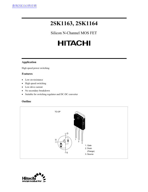
1. Gate 2. Drain (Flange) 3. Source
Page Summary Contents For HITACHI 2SK1163, 2SK1164 Silicon N-Channel MOS FET Data Manual
Manual Details
| Brand | Hitachi |
|---|---|
| Pages | 6 |
| File Size | 29.99 KB |
| Published | June 05, 2026 |
Enter the captcha to get the download link:

Frequently Asked Questions
What are the primary features of these power switching FETs?
They feature low on-resistance, high speed switching capability, and a low drive current.
What is the maximum allowable drain current (continuous)?
The maximum continuous Drain Current (ID) rating is 11 Amperes at Ta = 25°C.
How should I proceed if this product is used in mission-critical applications?
Contact Hitachi’s sales office before use in life support or high reliability fields like aerospace, as failure may cause bodily injury.
What package type and pin labeling are used for the components?
The outline is TO-3P. The pins are labeled 1 for Gate, 2 for Drain, and 3 for Source.