HITACHI 2SJ244 Silicon P-Channel MOS FET Data Sheet
Summary
This power MOSFET is engineered for high-speed efficiency in switching and motor driving circuits. Its robust design makes it ideal for applications such as camera or VTR motor drives, general power switches, and solenoid actuation systems requiring low voltage operation. The accompanying manual provides comprehensive technical specifications, including absolute maximum ratings, detailed thermal analysis curves, and crucial electrical parameters like on-resistance and switching times. It is essential documentation for electronics engineers and designers specifying reliable, high-performance components for demanding electromechanical applications.
Page 1 Text Content
查询2SJ244供应商
2SJ244 Silicon P-Channel MOS FET
Application
High speed power switching
Low voltage operation
Features
• Very Low on-resistance • High speed switching • Suitable for camera or VTR motor drive circuit, power switch, solenoid drive and etc.
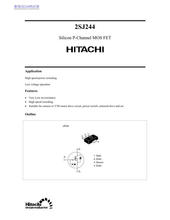
Outline
1. Gate 2. Drain 3. Source 4. Drain
Page Summary Contents For HITACHI 2SJ244 Silicon P-Channel MOS FET Data Sheet
Manual Details
| Brand | Hitachi |
|---|---|
| Pages | 8 |
| File Size | 41.30 KB |
| Published | June 03, 2026 |
Enter the captcha to get the download link:

Frequently Asked Questions
What is the maximum drain peak current allowed?
The absolute maximum rating for drain peak current (ID(pulse)) is -4A.
How does dissipation limit relate to ambient temperature?
Channel power dissipation (Pch) is limited by Rds(on) and performance chart, with specific operating modes defined for the alumina ceramic board.
What are the relevant switching delay times?
The turn-on delay time (t(d(on))) is 365 ns, and the turn-off delay time (t(d(off))) is 1450 ns.