HITACHI 2SJ172 Silicon P-Channel MOS FET Data Sheet
Summary
This comprehensive datasheet is perfect for electrical engineers and circuit designers requiring high-performance power components. It details the 2SJ172 Silicon P-Channel MOS FET, a robust switch known for its low on-resistance and high-speed switching capabilities. The manual provides exhaustive technical specifications, including maximum ratings, detailed electrical characteristics, and graphs covering various operational modes (e.g., DC operation, pulsing). Ideal for applications such as motor drives, DC-DC converters, and general power switching systems requiring reliability and efficiency.
Page 1 Text Content
查询2SJ172供应商
2SJ172 Silicon P-Channel MOS FET
November 1996
Application
High speed power switching
Features
• Low on-resistance • High speed switching • Low drive current • 4 V gate drive device Can be driven from 5 V source • Suitable for motor drive, DC-DC converter, power switch and solenoid drive
Outline
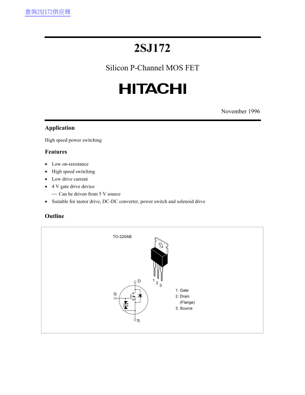
TO-220AB
1. Gate 2. Drain (Flange) 3. Source
Page Summary Contents For HITACHI 2SJ172 Silicon P-Channel MOS FET Data Sheet
Manual Details
| Brand | Hitachi |
|---|---|
| Pages | 7 |
| File Size | 37.19 KB |
| Published | June 03, 2026 |
Enter the captcha to get the download link:

Frequently Asked Questions
What power applications is the 2SJ172 transistor suitable for?
It is specified for use in motor drive, DC-DC converter, power switch, and solenoid drive applications.
What are the key switching voltage requirements for this FET?
The device requires a 4 V gate drive but can be driven from a standard 5 V source.
How fast is the transistor's switching performance?
The datasheet lists the rise time (t_r) at 65 ns and the fall time (t_f) at 105 ns.
What are the general operational limits regarding current and heat?
It has a maximum drain current of -10 A, and its channel dissipation is rated up to 40 W.