HITACHI 2SJ247 Silicon P-Channel MOS FET Data Sheet
Summary
This P-Channel MOS FET is engineered for high-speed precision power switching, making it ideal for building efficient DC-DC converters and switching regulator circuits. Featuring low on-resistance and minimal drive current, it ensures reliable performance in demanding power management applications. This technical manual provides comprehensive electrical characteristics, detailed operational limits, and extensive graphs required by engineers and designers integrating the FET into their power electronic systems.
Page 1 Text Content
查询2SJ247供应商
2SJ247 Silicon P-Channel MOS FET
Application
High speed power switching
Features
• Low on-resistance • High speed switching • Low drive current • 4 V gate drive device can be driven from 5 V source • Suitable for switching regulator, DC-DC converter
Outline
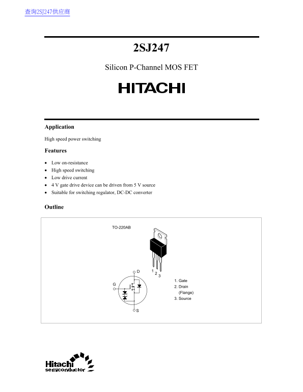
TO-220AB
1. Gate 2. Drain (Flange) 3. Source
Page Summary Contents For HITACHI 2SJ247 Silicon P-Channel MOS FET Data Sheet
Manual Details
| Brand | Hitachi |
|---|---|
| Pages | 8 |
| File Size | 43.21 KB |
| Published | June 03, 2026 |
Enter the captcha to get the download link:

Frequently Asked Questions
What is the maximum typical dissipation power of this FET when Ta = 25°C?
The channel dissipation Pch* at 25°C is rated at up to 40 W.
Is 2SJ247 suitable for switching regulators or DC-DC converters?
Yes, the device features make it suitable for use in switching regulators and DC-DC converters.
How low can the on-resistance be at a given voltage?
The static drain to source on state resistance (R(on)) is typically 0.3 Ohms when I = –4 A and V = –10 V.
What is the recommended method for limiting power over time?
When operating in a pulse test scenario, consider the Normalized Transient Thermal Impedance vs. Pulse Width graph to ensure safe operation (PW).