# A B C D E F G H I J K L M N O P Q R S T U V W X Y Z

HITACHI 2SJ319(L),2SJ319(S) Data Sheet

Summary

Master this power switching challenge with the 2SJ319 P-Channel MOS FETs. This component is engineered for high-speed power applications, offering low on-resistance and robust performance in circuits like DC-DC converters and switching regulators. The datasheet provides comprehensive technical specifications, including electrical characteristics, maximum ratings across various temperatures, and detailed analysis of switching transients. Designed for power electronics engineers and circuit designers who require reliable, efficient component data for advanced hardware development.
📄 Preview PAGE OF 10

Page 1 Text Content

查询2SJ319供应商

2SJ319(L), 2SJ319(S) Silicon P-Channel MOS FET

Application

High speed power switching

Features

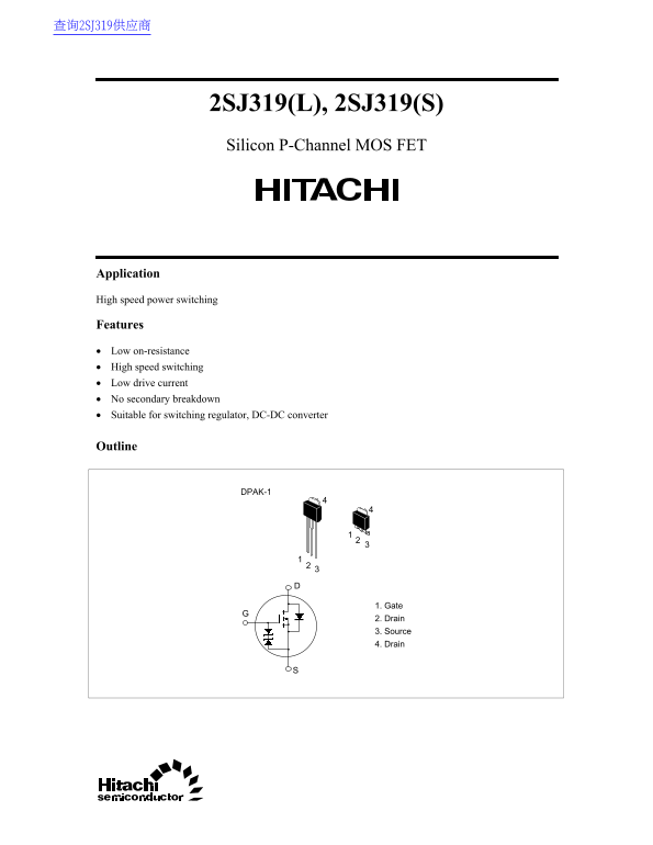
• Low on-resistance • High speed switching • Low drive current • No secondary breakdown • Suitable for switching regulator, DC-DC converter

Outline

DPAK-1

1. Gate 2. Drain 3. Source 4. Drain

Page Summary Contents For HITACHI 2SJ319(L),2SJ319(S) Data Sheet

Page 1 查询2SJ319供应商 2SJ319(L), 2SJ319(S) Silicon P-Channel MOS FET Application High speed power switching Features • Low on-resistance • High speed switching • Low drive current • No secondary breakdown • Sui...
Page 2 2SJ319(L), 2SJ319(S) Absolute Maximum Ratings (Ta = 25°C) Item Symbol Ratings Unit Drain to source voltage VDSS –200 Gate to source voltage VGSS ±20 Drain current ID –3 Drain peak current ID(pulse)* –...
Page 3 2SJ319(L), 2SJ319(S) ha nn el is si pa tio ch ra in ur re nt Power vs. Temperature Derating Maximum Safe Operation Area 10 µs 100 µs PW –3 1 ms DC Operation (Tc = 25 °C) = 10 ms (1shot)Operation in –0...
Page 4 2SJ319(L), 2SJ319(S) ra in to ou rc at ur at io ol ta ge ta tic ra in to ou rc on ta te es is ta nc Static Drain to Source on State Resistance (o n) (o n) Drain to Source Saturation Voltage vs. Gate t...
Page 5 2SJ319(L), 2SJ319(S) ev er se ec ov er im rr ns ra in to ou rc ol ta ge Typical Capacitance vs. Body–Drain Diode Reverse Drain to Source Voltage Recovery Time V = 0 GS f = 1 MHz di/dt = 50 A/µs, V = 0...
Page 6 2SJ319(L), 2SJ319(S) or Reverse Drain Current vs. al iz ed ra ns ie nt he rm al Im pe da nc Source to Drain Voltage t) –5 Pulse Test –4 ev er se ra in ur re nt (A V = 0, 5 VGS –0.4 –0.8 –1.2 –1.6 –2 S...
Page 7 2SJ319(L), 2SJ319(S) Switching Time Test Circuit Waveforms Vin Monitor Vout Monitor Vin DD 10% 10%Vout td(off) tf trtd(on)
Page 8 Unit: mm Hitachi Code DPAK (L)-(1) JEDEC EIAJ Conforms Weight (reference value) 0.42 g
Page 9 Cautions 1. Hitachi neither warrants nor grants licenses of any rights of Hitachi’s or any third party’s patent, copyright, trademark, or other intellectual property rights for information contained i...
Page 10 WWW.ALLDATASHEET.COM Copyright © Each Manufacturing Company. All Datasheets cannot be modified without permission. This datasheet has been download from : www.All Data Sheet.com 100% Free Data Sheet S...

Manual Details

Brand Hitachi
Pages 10
File Size 46.32 KB
Published June 03, 2026
29 views

Enter the captcha to get the download link:

captcha

Frequently Asked Questions

What is the maximum drain to source voltage (DSS) rating?

The absolute maximum rating for Drain to Source Voltage is -200 V.

What current limitations should I consider when running high power?

Always check the Power vs. Temperature Derating area, as it limits operation based on R_DS(on).

What are the key performance features for switching applications?

It offers low on-resistance, high speed switching, and is suitable for use in switching regulators or DC-DC converters.

How does temperature affect the maximum drain current rating?

The maximum safe area requires checking the power vs. temperature derating curve to ensure reliable operation.