# A B C D E F G H I J K L M N O P Q R S T U V W X Y Z

HITACHI 2SJ221 Data Sheet

Summary

The 2SJ221 is a high-speed Silicon P-Channel MOS FET designed for robust power switching in demanding applications such as motor drives, DC-DC converters, and solenoids. This comprehensive technical manual serves professional engineers and circuit designers by providing critical specifications, including absolute maximum ratings, detailed electrical characteristics (Rds(on), capacitances), and thermal performance graphs. Use this guide to ensure optimal selection and reliable high-power switching design implementation.
📄 Preview PAGE OF 8

Page 1 Text Content

查询2SJ221供应商

2SJ221 Silicon P-Channel MOS FET

Application

High speed power switching

Features

• Low on-resistance • High speed switching • Low drive current • 4 V gate drive device  Can be driven from 5 V source • Suitable for motor drive, DC-DC converter, power switch and solenoid drive

Outline

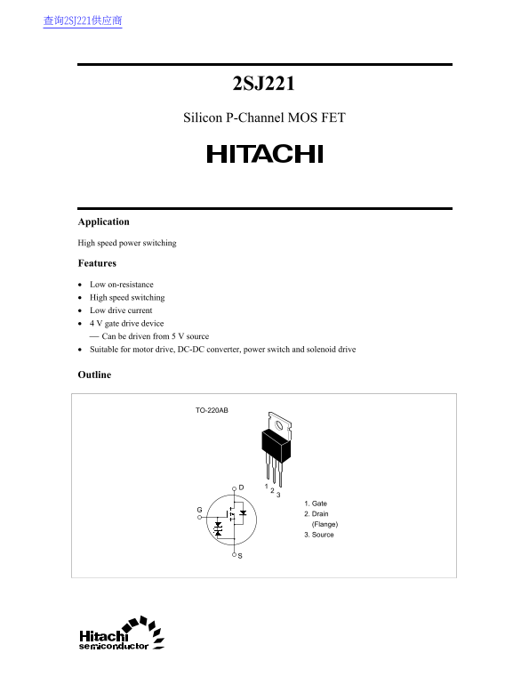
TO-220AB

1. Gate 2. Drain (Flange) 3. Source

Page Summary Contents For HITACHI 2SJ221 Data Sheet

Page 1 查询2SJ221供应商 2SJ221 Silicon P-Channel MOS FET Application High speed power switching Features • Low on-resistance • High speed switching • Low drive current • 4 V gate drive device  Can be driven from...
Page 2 2SJ221 Absolute Maximum Ratings (Ta = 25°C) Item Symbol Ratings Unit Drain to source voltage VDSS –100 Gate to source voltage VGSS ±20 Drain current ID –20 Drain peak current ID(pulse)* –80 Body to dr...
Page 3 2SJ221 ha nn el is si pa tio ch ra in ur re nt Power vs. Temperature Derating Maximum Safe Operation Area –100 s DC Operation (T s (1 Shot) C = 25°C) –3 Ta = 25°C –0.3 Operation in this Area is Limite...
Page 4 2SJ221 ra in to ou rc at ur at io ol ta ge (V ta tic ra in to ou rc on ta te es is ta nc Drain to Source Saturation Voltage Static Drain to Source on State (Ω on vs. Gate to Source Voltage Resistance ...
Page 5 2SJ221 ra in to ou rc ol ta ge ev er se ec ov er im s) Body to Drain Diode Reverse Typical Capacitance vs. Recovery Time Drain to Source Voltage 3,000 di/dt = 50 A/µs, Ta = 25°C VGS = 0 VGS = 0, f = 1...
Page 6 2SJ221 or al iz ed ra ns ie nt he rm al Im pe da nc t) Reverse Drain Current vs. Source to Drain Voltage Pulse Test –40 ev er se ra in ur re nt VGS = 0, 5 V Source to Drain Voltage VSD (V) Normalized ...
Page 7 Unit: mm 11.5 MAX 2.7 MAX 1.5 MAX Hitachi Code TO-220AB JEDEC Conforms EIAJ Conforms Weight (reference value) 1.8 g
Page 8 Cautions 1. Hitachi neither warrants nor grants licenses of any rights of Hitachi’s or any third party’s patent, copyright, trademark, or other intellectual property rights for information contained i...

Manual Details

Brand Hitachi
Pages 8
File Size 44.18 KB
Published June 05, 2026
27 views

Enter the captcha to get the download link:

captcha

Frequently Asked Questions

What is the maximum continuous power dissipation?

The maximum channel dissipation ($P_{ch*}$) for this FET is $75 ext{ W}$.

What are the absolute voltage limitations?

The Drain to source voltage rating ($V_{DSS}$) is $-100 ext{ V}$, and the Gate to source ($V_{GSS}$) is $-20 ext{ V}.

How fast can this FET switch, and what limits its operation?

It offers high-speed switching. However, operation in certain areas is limited by the on-resistance ($R_{DS(on)}$).