HITACHI 2SJ217 Data Sheet
Summary
The 2SJ217 is a robust P-Channel MOS FET engineered for demanding power switching applications requiring high efficiency and rapid response time. It excels in motor drives, DC-DC converters, and general power switch systems due to its low on-resistance and low drive current. This manual serves as the definitive guide, detailing comprehensive technical specifications, absolute maximum ratings, electrical characteristics (including detailed capacitance and switching times), thermal derating curves, and operational limits essential for professional circuit design and system integration.
Page 1 Text Content
查询2SJ217供应商
2SJ217 Silicon P-Channel MOS FET
November 1996
Application
High speed power switching
Features
• Low on-resistance • High speed switching • Low drive current • 4 V gate drive device Can be driven from 5 V source • Suitable for motor drive, DC-DC converter, power switch and solenoid drive
Outline
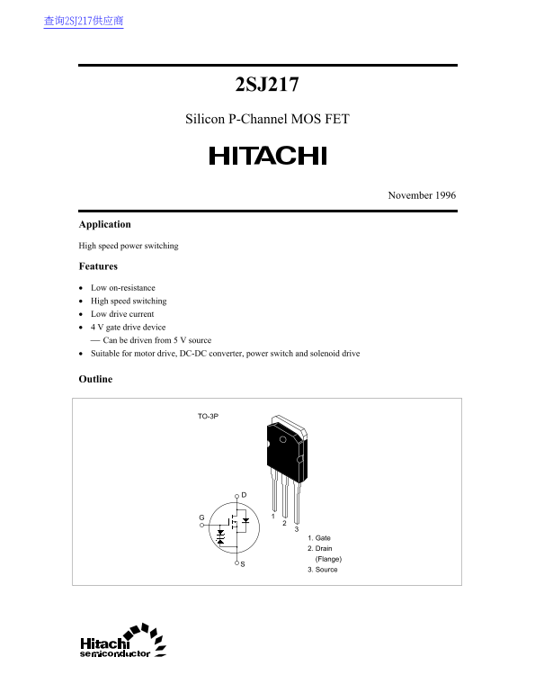
TO-3P
1. Gate 2. Drain (Flange) 3. Source
Page Summary Contents For HITACHI 2SJ217 Data Sheet
Manual Details
| Brand | Hitachi |
|---|---|
| Pages | 9 |
| File Size | 45.39 KB |
| Published | June 03, 2026 |
Enter the captcha to get the download link:

Frequently Asked Questions
What is the maximum power dissipation for this device?
The average channel dissipation (Pch) is rated at 150 W.
Can I use this FET for DC-DC converters or motor drives?
Yes, it is suitable for motor drive, DC-DC converter, power switch, and solenoid drive applications.
What are the absolute voltage ratings for the gate to source connection?
The maximum Gate to source overvoltage (V GSS) rating is –20 V.
How does the device perform in high temperature environments?
It features a Maximum Safe Operation Area chart allowing calculation of operation limits based on case and ambient temperatures.
What is the typical On-State Resistance (R DS(on))?
At I = –20 A, V = –10 V*, the typical R DS(on) value is 0.042 Ohm.