FAIRCHILD KSD261 NPN Epitaxial Silicon Transistor User Manual
Summary
Optimize your electronics design with the KSD261, a reliable NPN low-frequency power amplifier transistor. This technical datasheet serves as a comprehensive resource for electrical engineers and circuit designers requiring precise component specifications. It details absolute maximum ratings, detailed current gain curves (hFE), saturation voltages, and performance characteristics necessary for stable signal amplification in low-power applications. Use this manual to model and ensure the effective integration of the KSD261 into high-performance power circuits.
Page 1 Text Content
KSD261
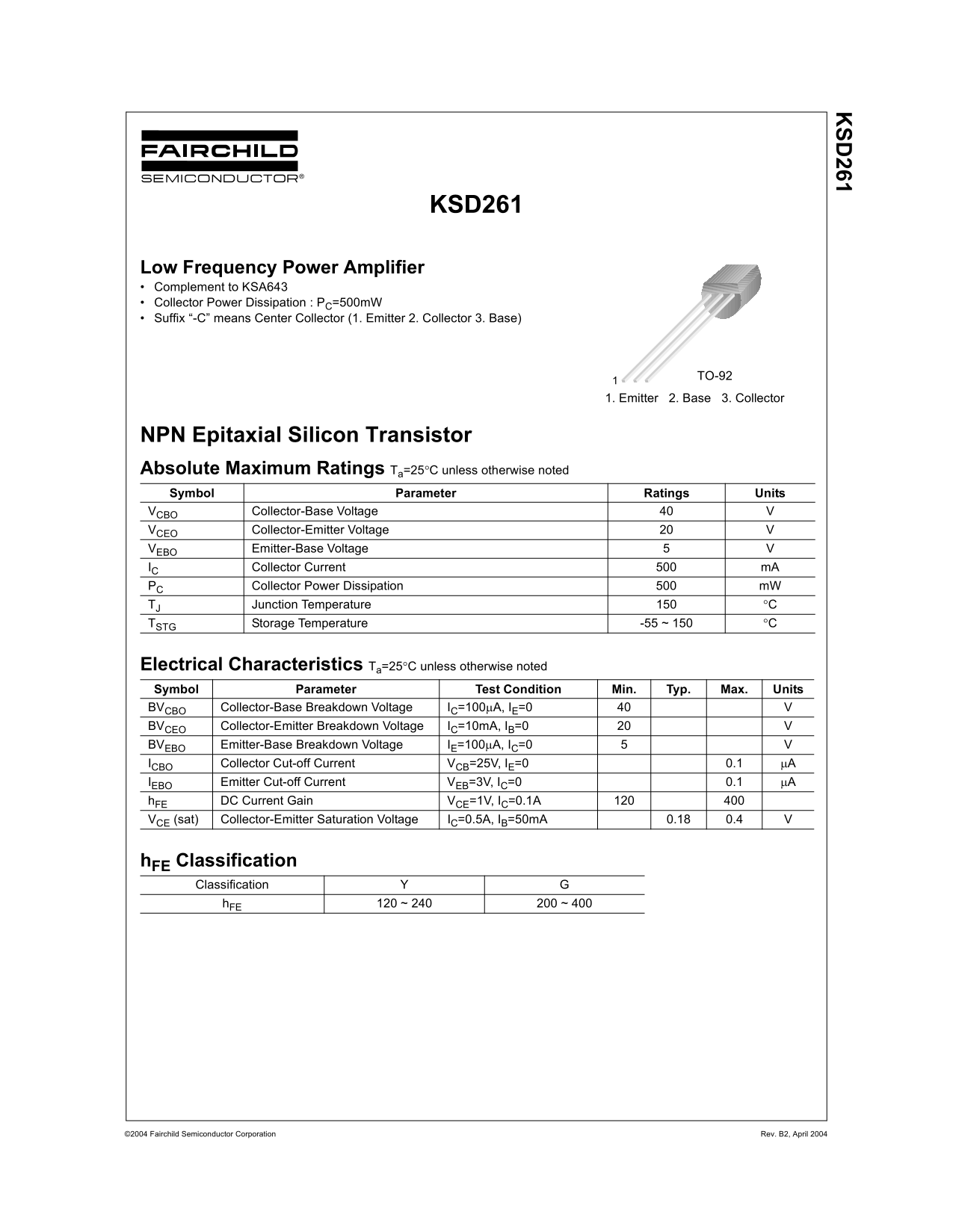
Low Frequency Power Amplifier Complement to KSA643 Collector Power Dissipation : PC=500m W Suffix “-C” means Center Collector (1. Emitter 2. Collector 3. Base)
TO-921
1. Emitter 2. Base 3. Collector
NPN Epitaxial Silicon Transistor Absolute Maximum Ratings Ta=25°C unless otherwise noted Symbol Parameter Ratings Units VCBO Collector-Base Voltage
VCEO Collector-Emitter Voltage VEBO Emitter-Base Voltage IC Collector Current m A PC Collector Power Dissipation m W TJ Junction Temperature °C TSTG Storage Temperature -55 ~ 150 °C
Electrical Characteristics Ta=25°C unless otherwise noted Symbol Parameter Test Condition Min. Typ. Max. Units BVCBO Collector-Base Breakdown Voltage IC=100µA, IE=0
BVCEO Collector-Emitter Breakdown Voltage IC=10m A, IB=0 BVEBO Emitter-Base Breakdown Voltage IE=100µA, IC=0 ICBO Collector Cut-off Current VCB=25V, IE=0 0.1 µA IEBO Emitter Cut-off Current VEB=3V, IC=0 0.1 µA h FE DC Current Gain VCE=1V, IC=0.1A VCE (sat) Collector-Emitter Saturation Voltage IC=0.5A, IB=50m A 0.18 0.4
h FE Classification Classification Y
h FE 120 ~ 240 200 ~ 400
©2004 Fairchild Semiconductor Corporation Rev. B2, April 2004
Page Summary Contents For FAIRCHILD KSD261 NPN Epitaxial Silicon Transistor User Manual
Manual Details
| Brand | Fairchild |
|---|---|
| Pages | 4 |
| File Size | 39.11 KB |
| Published | July 07, 2026 |
Enter the captcha to get the download link:

Frequently Asked Questions
What is the maximum allowed operating voltage for the collector-emitter junction?
The absolute maximum rating for Collector-Emitter Voltage (CEO) is 20V.
Can I use this transistor in life support medical devices?
No, Fairchild's products are not authorized for use as critical components in life support devices without express written approval.
What is the typical DC Current Gain (hFE)?
At a collector current of 10mA, the DC Current Gain hFE typically ranges from 120 to 240.
Does this datasheet represent final specifications for purchasing?
Only a datasheet labeled 'Full Production' contains final specifications; preliminary data requires supplementary publications.