Fairchild FJY3014R NPN Epitaxial Silicon Transistor Data Handbook
Summary
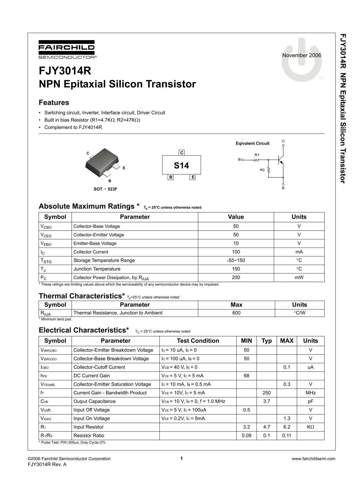
This datasheet from Fairchild Semiconductor covers the FJY3014R NPN epitaxial silicon transistor with built-in bias resistors of 4.7 kilohms and 47 kilohms, complementing the FJY4014R PNP type. Packaged in the compact SOT-523F surface-mount outline, it is intended for switching circuits, inverter, interface, and driver circuit applications. Key specifications include a collector-emitter breakdown voltage of 50 V, maximum collector current of 100 mA, DC current gain of 68 minimum at 5 V and 5 mA,
Page 1 Text Content
FJY3014R PN Epitaxial Silicon Transistor
November 2006
FJY3014R
NPN Epitaxial Silicon Transistor Features Switching circuit, Inverter, Interface circuit, Driver Circuit Built in bias Resistor (R1=4.7KΩ, R2=47KΩ) Complement to FJY4014R
Eqivalent Circuit
SOT - 523F
Absolute Maximum Ratings * Ta = 25°C unless otherwise noted Symbol Parameter Value Units VCBO Collector-Base Voltage 50 VCEO Collector-Emitter Voltage 50 VEBO Emitter-Base Voltage 10 IC Collector Current 100 m A TSTG Storage Temperature Range -55~150 °C TJ Junction Temperature °C PC Collector Power Dissipation, by RθJA m W * These ratings are limiting values above which the serviceability of any semiconductor device may by impaired.
Thermal Characteristics* Ta=25°C unless otherwise noted Symbol Parameter Max Units RθJA Thermal Resistance, Junction to Ambient °C/W * Minimum land pad.
Electrical Characteristics* TC = 25°C unless otherwise noted Symbol Parameter Test Condition MIN Typ MAX Units V(BR)CBO Collector-Emitter Breakdown Voltage IC = 10 u A, IE = 0 V(BR)CEO Collector-Base Breakdown Voltage IC = 100 u A, IB = 0 ICBO Collector-Cutoff Current VCB = 40 V, IE = 0 0.1 u A h FE DC Current Gain VCE = 5 V, IC = 5 m A VCE(sat) Collector-Emitter Saturation Voltage IC = 10 m A, IB = 0.5 m A 0.3 f T Current Gain - Bandwidth Product VCE = 10V, IC = 5 m A MHz Ccb Output Capacitance VCB = 10 V, IE = 0, f = 1.0 MHz 3.7 p F VI(off) Input Off Voltage VCE = 5 V, IC = 100u A 0.5 VI(on) Input On Voltage VCE = 0.2V, IC = 5m A 1.3 R1 Input Resistor 3.2 4.7 6.2 KΩ R1/R2 Resistor Ratio 0.09 0.1 0.11 * Pulse Test: PW≤300µs, Duty Cycle≤2%
©2006 Fairchild Semiconductor Corporation www.fairchildsemi.com FJY3014R Rev. A
Page Summary Contents For Fairchild FJY3014R NPN Epitaxial Silicon Transistor Data Handbook
Manual Details
| Brand | Fairchild |
|---|---|
| Pages | 4 |
| File Size | 312.73 KB |
| Published | July 07, 2026 |
Enter the captcha to get the download link:

Frequently Asked Questions
What is the maximum collector power dissipation?
Power dissipation (PC) is limited to 200 mW when using an ambient temperature of 25°C.
Is this transistor suitable for life support applications?
No, Fairchild's products are not authorized for use as critical components in life support devices without explicit written approval.
What kind of signals does the FJY3014R Transistor handle?
It is designed for switching circuits, inverters, interface circuits, and driver circuits.
What is the junction temperature range?
The Junction Temperature (TJ) must remain below 150°C.