Fairchild FQAF33N10L Specifications Sheet
Summary
This datasheet provides comprehensive specifications for the FQAF33N10L N-Channel MOSFET—a high-performance power transistor ideal for demanding switching applications. Engineered for superior efficiency, the device features low $\text{R}_{\mathrm{DS(on)}}$ and fast switching characteristics, making it perfect for high-efficiency DC/DC converters and advanced DC motor control systems. The document details crucial electrical ratings, thermal profiles, and operating parameters required by electronics designers to ensure reliable circuit design and peak performance in power management applications.
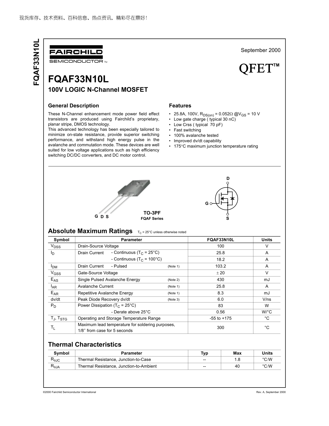
Page 1 Text Content
September 2000
QFETTM
FQAF33N10L 100V LOGIC N-Channel MOSFET General Description Features These N-Channel enhancement mode power field effect 25.8A, 100V, RDS(on) = 0.052Ω @VGS = 10 V transistors are produced using Fairchild’s proprietary, Low gate charge ( typical 30 n C) planar stripe, DMOS technology. Low Crss ( typical 70 p F) This advanced technology has been especially tailored to Fast switching minimize on-state resistance, provide superior switching 100% avalanche tested performance, and withstand high energy pulse in the
Improved dv/dt capability
avalanche and commutation mode. These devices are well
175°C maximum junction temperature rating
suited for low voltage applications such as high efficiency switching DC/DC converters, and DC motor control.
TO-3PF
FQAF Series G
Absolute Maximum Ratings TC = 25°C unless otherwise noted Symbol Parameter FQAF33N10L Units VDSS Drain-Source Voltage ID Drain Current - Continuous (TC = 25°C) 25.8
- Continuous (TC = 100°C) 18.2
IDM Drain Current - Pulsed (Note 1) 103.2 VGSS Gate-Source Voltage ± 20 EAS Single Pulsed Avalanche Energy (Note 2) m J IAR Avalanche Current (Note 1) 25.8 EAR Repetitive Avalanche Energy (Note 1) 8.3 m J
dv/dt Peak Diode Recovery dv/dt (Note 3) 6.0 V/ns
PD Power Dissipation (TC = 25°C)
- Derate above 25°C 0.56 W/°C
TJ, TSTG Operating and Storage Temperature Range -55 to +175 °C
Maximum lead temperature for soldering purposes,
TL °C
1/8" from case for 5 seconds
Thermal Characteristics Symbol Parameter Typ Max Units RθJC Thermal Resistance, Junction-to-Case 1.8 °C/W RθJA Thermal Resistance, Junction-to-Ambient °C/W
©2000 Fairchild Semiconductor International Rev. A, September 2000
Page Summary Contents For Fairchild FQAF33N10L Specifications Sheet
Manual Details
| Brand | Fairchild |
|---|---|
| Pages | 8 |
| File Size | 662.96 KB |
| Published | July 07, 2026 |
Enter the captcha to get the download link:

Frequently Asked Questions
What is the continuous drain current of this device at room temperature (25°C)?
The maximum continuous drain current (IDSS) is 25.8 A.
What type of applications are these N-Channel MOSFETs best suited for?
They are suitable for low voltage applications such as high efficiency switching DC/DC converters and DC motor control.
Is there a maximum operating temperature limit for this component?
The device has an operating temperature range of -55 to +175°C.
What is the recommended on-resistance (Rds(on)) specification at standard testing conditions?
The typical on-resistance is 0.052 Ω at 25°C.