# A B C D E F G H I J K L M N O P Q R S T U V W X Y Z

Fairchild AN6012 Specifications Sheet

Summary

Application note AN6012 from Fairchild Semiconductor detailing design of power factor correction (PFC) circuit using FAN7528 voltage mode critical conduction mode (CRM) boost PFC controller. Explains CRM PFC operation at boundary of continuous and discontinuous conduction modes, where switch turn-on occurs when inductor current reaches zero and turn-off determined by internal ramp signal compared with error amplifier output. Constant turn-on time ensures inductor peak current proportional to rec
📄 Preview 📖 Table of Contents Contents PAGE OF 15

Page 1 Text Content

www.fairchildsemi.com

Application Note AN6012 Design of Power Factor Correction Circuit Using FAN7528

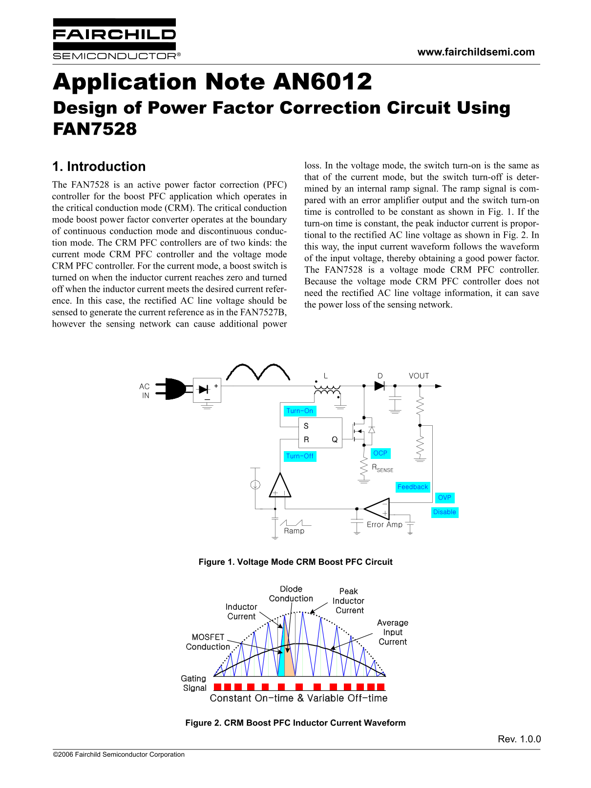
1. Introduction loss. In the voltage mode, the switch turn-on is the same as that of the current mode, but the switch turn-off is deter-

The FAN7528 is an active power factor correction (PFC)

mined by an internal ramp signal. The ramp signal is com-

controller for the boost PFC application which operates in

pared with an error amplifier output and the switch turn-on

the critical conduction mode (CRM). The critical conduction

time is controlled to be constant as shown in Fig. 1. If the

mode boost power factor converter operates at the boundary

turn-on time is constant, the peak inductor current is propor-

of continuous conduction mode and discontinuous conduc-

tional to the rectified AC line voltage as shown in Fig. 2. In

tion mode. The CRM PFC controllers are of two kinds: the

this way, the input current waveform follows the waveform

current mode CRM PFC controller and the voltage mode

of the input voltage, thereby obtaining a good power factor.

CRM PFC controller. For the current mode, a boost switch is

The FAN7528 is a voltage mode CRM PFC controller.

turned on when the inductor current reaches zero and turned

Because the voltage mode CRM PFC controller does not

off when the inductor current meets the desired current refer-

need the rectified AC line voltage information, it can save

ence. In this case, the rectified AC line voltage should be

the power loss of the sensing network.

sensed to generate the current reference as in the FAN7527B, however the sensing network can cause additional power

AC IN

Turn-On

Turn-Off

RSENSE

Feedback

Disable

Error Amp

Figure 1. Voltage Mode CRM Boost PFC Circuit

Diode

Conduction

Inductor Current Inductor

Current

Average Input

MOSFET

Current

Conduction

Gating Signal

Constant On-time & Variable Off-time

Figure 2. CRM Boost PFC Inductor Current Waveform

Rev. 1.0.0

©2006 Fairchild Semiconductor Corporation

Page Summary Contents For Fairchild AN6012 Specifications Sheet

Page 1 www.fairchildsemi.com Application Note AN6012 Design of Power Factor Correction Circuit Using FAN7528 1. Introduction loss. In the voltage mode, the switch turn-on is the same as that of the current m...
Page 2 AN6012 APPLICATION NOTE Unlike the conventional fixed output CRM PFC controllers, used to get the information of the AC line voltage range, the FAN7528 has the dual output control function according w...
Page 3 APPLICATION NOTE AN6012 Figure 5. FAN7528 Start-up Waveform When 264Vac Fig. 6 shows the block diagram of the FAN7528. Vcc Vref UVLO Vcc Internal Bias 12V 8.5V Disable OUTDrive Output 160us Timer Zero...
Page 4 AN6012 APPLICATION NOTE 2. Device Block Description converter, Vcc voltage starts to increase from zero voltage. If the Vcc voltage reaches 8.5V, the dual output reference gen- 2.1 Error Amplifier Blo...
Page 5 APPLICATION NOTE AN6012 2.2 Zero Current Detection Block voltage becomes positive and proportional to the difference between Vout and Vin. If the inductor current reaches zero, The zero current detect...
Page 6 AN6012 APPLICATION NOTE Figure 10. Current Flow During tzero In the ZCD block, there is an internal timer to provide a turn-off instant. The slope of the saw tooth is determined by means to start or r...
Page 7 APPLICATION NOTE AN6012 3.Circuit Components Design 3) Input Capacitor Design 3.1 Power Stage Design The voltage ripple of the input capacitor is maximum when the line is lowest and the load is heavie...
Page 8 AN6012 APPLICATION NOTE ai Ai PFC Ci AV a V Circuit Input Filter Figure 14. Input Voltage and Current Displacement Due to Input Filter Capacitance 4) Output Capacitor Design IO The output capacitor is...
Page 9 APPLICATION NOTE AN6012 3.2 Control Circuit Design 1) Output Voltage Sensing Resistor and Feedback Loop Design The output voltage sensing resistors, R1 and R2 are deter- mined by the output voltage at...
Page 10 AN6012 APPLICATION NOTE of the AC line as shown in Fig. 21. To minimize the zero crossing distortion, Coss must be minimized and a larger inductor should be used. But there is a limitation in minimiz-...
Page 11 APPLICATION NOTE AN6012 Ramp Slope Change Vac Slope Decrease Slope Increase Variable On-time On-time Increase On-time Decrease Figure 23. On-time Variation according to Vac 3) Start-up Circuit Design ...
Page 12 AN6012 APPLICATION NOTE 4.5 Output Voltage Sense Resistor and 4.9 MOT Resistor Design Feedback Loop Design The MOT resistor is determined to get the maximum on-time The upper output voltage sense resi...
Page 13 APPLICATION NOTE AN6012 Table 2. 100W Demo Board Part List PART# VALUE NOTE PART# VALUE NOTE Fuse Capacitor F1 250V/3A C1 150n F/275Vac Box Capacitor TNR C2 330n F/275Vac Box Capacitor V1 470V C3,C4 2...
Page 14 AN6012 APPLICATION NOTE Nomenclature IL(peak) (t): inductor current peak value during one switching fac: AC line frequency cycle ω: AC line angular frequency IL(peak): inductor current peak value duri...
Page 15 AN6012 APPLICATION NOTE DISCLAIMER FAIRCHILD SEMICONDUCTOR RESERVES THE RIGHT TO MAKE CHANGES WITHOUT FURTHER NOTICE TO ANY PRODUCTS HEREIN TO IMPROVE RELIABILITY, FUNCTION OR DESIGN. FAIRCHILD DOES N...