Fairchild FDD3680 Product Specifications Sheet
Summary
Boost system efficiency with the FDD3680 N-Channel MOSFET, a high-performance component engineered for DC/DC power conversion circuits. Featuring ultra-low R DS(ON), fast switching response, and low gate charge, this device improves overall energy efficiency in synchronous or conventional PWM converter designs. This comprehensive manual provides all necessary electrical specifications, including absolute maximum ratings, thermal characteristics, switching parameters, and current capabilities required by electrical and hardware engineers designing high-power, reliable supply systems.
Page 1 Text Content
February 2001
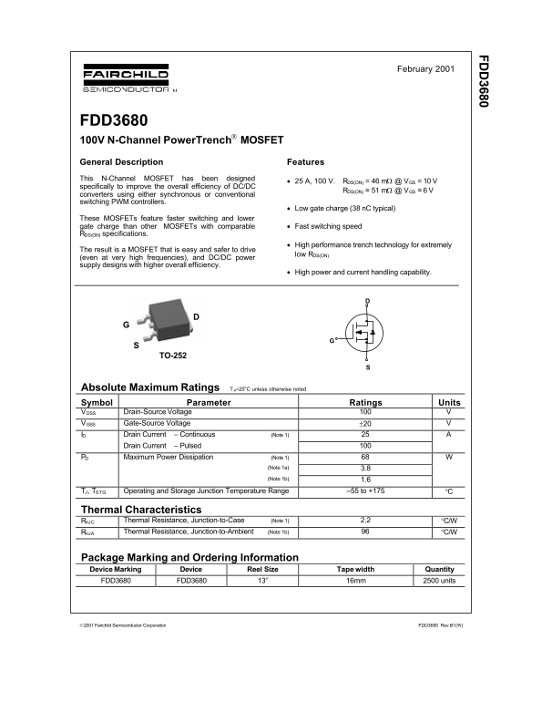
FDD3680 100V N-Channel Power Trench MOSFET General Description Features This N-Channel MOSFET has been designed
• 25 A, 100 V. RDS(ON) = 46 mΩ @ VGS = 10 V
specifically to improve the overall efficiency of DC/DC
RDS(ON) = 51 mΩ @ VGS = 6 V
converters using either synchronous or conventional switching PWM controllers.
• Low gate charge (38 n C typical)
These MOSFETs feature faster switching and lower gate charge than other MOSFETs with comparable • Fast switching speed RDS(ON) specifications.
• High performance trench technology for extremely
The result is a MOSFET that is easy and safer to drive
low RDS(ON)
(even at very high frequencies), and DC/DC power supply designs with higher overall efficiency.
• High power and current handling capability.
TO-252
Absolute Maximum Ratings T A=25o C unless otherwise noted
Symbol Parameter Ratings Units VDSS Drain-Source Voltage VGSS Gate-Source Voltage ±20 ID Drain Current – Continuous (Note 1)
Drain Current – Pulsed
PD Maximum Power Dissipation (Note 1)
(Note 1a) 3.8 (Note 1b) 1.6
TJ, TSTG Operating and Storage Junction Temperature Range –55 to +175 °C
Thermal Characteristics
RθJC Thermal Resistance, Junction-to-Case (Note 1) 2.2 °C/W RθJA Thermal Resistance, Junction-to-Ambient (Note 1b) °C/W
Package Marking and Ordering Information Device Marking Device Reel Size Tape width Quantity FDD3680 FDD3680 13’’ 16mm 2500 units
2001 Fairchild Semiconductor Corporation FDD3680 Rev B1(W)
Page Summary Contents For Fairchild FDD3680 Product Specifications Sheet
Manual Details
| Brand | Fairchild |
|---|---|
| Pages | 5 |
| File Size | 75.19 KB |
| Published | May 20, 2026 |
Enter the captcha to get the download link:

Frequently Asked Questions
What is the maximum continuous drain current for this MOSFET?
The maximum rated continuous drain current ($I_D$) is 25 A.
Can I use this component in a life support device?
No; Fairchild's products cannot be used as critical components in life support systems without express written approval.
What types of power converters is this MOSFET designed to optimize for?
It is specifically designed to improve DC/DC converters using synchronous or conventional switching PWM controllers.
How is the effective thermal resistance (R) calculated?
The resultant thermal resistance (R) is the sum of the junction-to-case ($R_{qJC}$) and case-to-ambient ($R_{CA}$) thermal resistance.