Fairchild FDG6335N 20v N-Channel PowerTrench MOSFET Data Manual
Summary
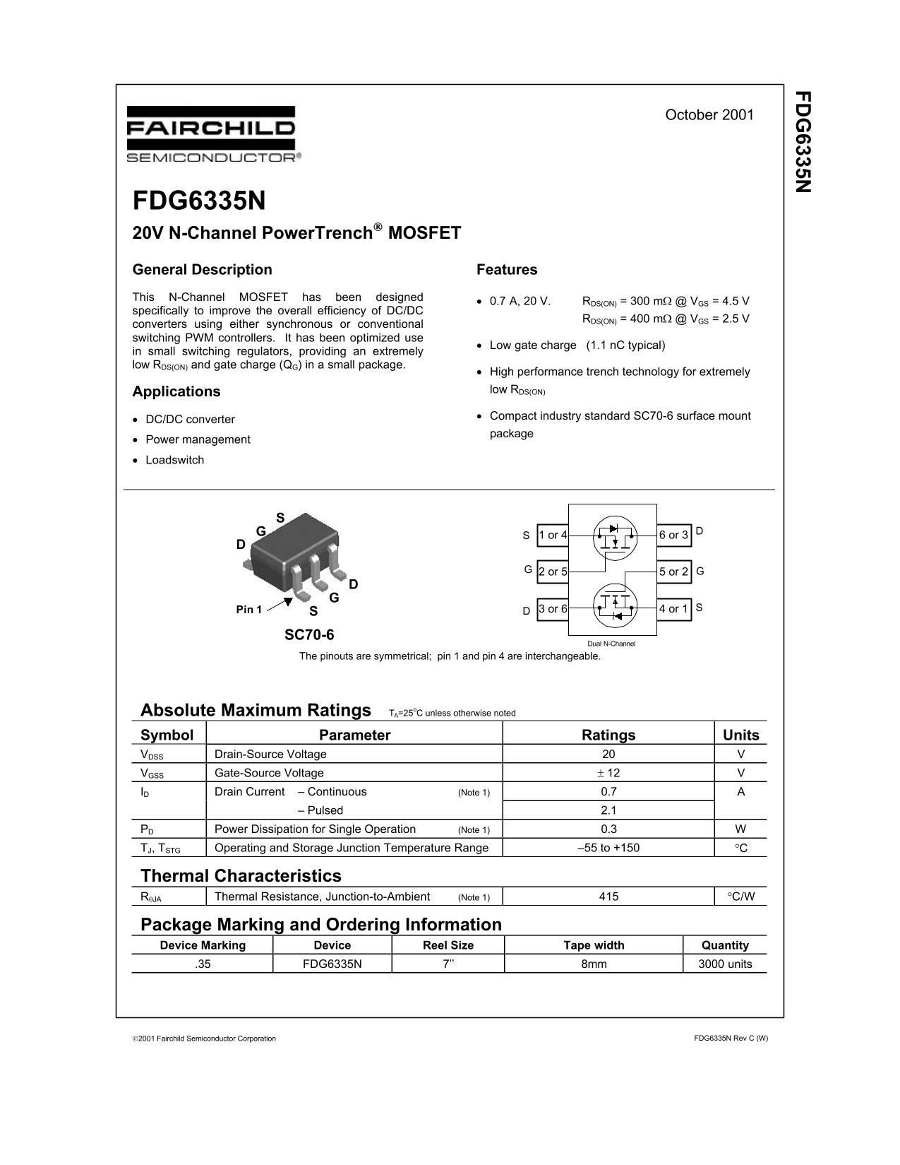
Datasheet for Fairchild FDG6335N dual N-Channel MOSFET in compact SC70-6 surface-mount package, specifically designed to improve overall efficiency of DC/DC converters using either synchronous or conventional switching PWM controllers. Features extremely low RDS(ON) resistance (400mΩ maximum at VGS = 4.5V, ID = 2.5A; 300mΩ maximum at VGS = 2.5V, ID = 2.0A) optimized for small switching regulators, very low gate charge (QG = 1.1nC typical at VGS = 4.5V), and high-performance trench technology for
Page 1 Text Content
October 2001
FDG6335N 20V N-Channel Power Trench MOSFET General Description Features This N-Channel MOSFET has been designed
• 0.7 A, 20 V. RDS(ON) = 300 mΩ @ VGS = 4.5 V
specifically to improve the overall efficiency of DC/DC
RDS(ON) = 400 mΩ @ VGS = 2.5 V
converters using either synchronous or conventional switching PWM controllers. It has been optimized use
• Low gate charge (1.1 n C typical)
in small switching regulators, providing an extremely low RDS(ON) and gate charge (QG) in a small package.
• High performance trench technology for extremely Applications low RDS(ON)
• Compact industry standard SC70-6 surface mount
• DC/DC converter
package
• Power management • Loadswitch
1 or 4 6 or 3
2 or 5 5 or 2
Pin 1 3 or 6 4 or 1
SC70-6
Dual N-Channel
The pinouts are symmetrical; pin 1 and pin 4 are interchangeable.
Absolute Maximum Ratings TA=25o C unless otherwise noted Symbol Parameter Ratings Units VDSS Drain-Source Voltage VGSS Gate-Source Voltage ± 12 ID Drain Current – Continuous (Note 1) 0.7
– Pulsed 2.1
PD Power Dissipation for Single Operation (Note 1) 0.3 TJ, TSTG Operating and Storage Junction Temperature Range –55 to +150 °C
Thermal Characteristics RθJA Thermal Resistance, Junction-to-Ambient (Note 1) °C/W
Package Marking and Ordering Information Device Marking Device Reel Size Tape width Quantity
.35 FDG6335N 7’’ 8mm 3000 units
2001 Fairchild Semiconductor Corporation FDG6335N Rev C (W)
Page Summary Contents For Fairchild FDG6335N 20v N-Channel PowerTrench MOSFET Data Manual
Manual Details
| Brand | Fairchild |
|---|---|
| Pages | 5 |
| File Size | 66.23 KB |
| Published | July 07, 2026 |
Enter the captcha to get the download link:

Frequently Asked Questions
What is the optimized use case for this MOSFET?
It is designed specifically to improve efficiency in DC/DC converters using synchronous or conventional switching PWM controllers.
What is the maximum continuous drain current (ID)?
The specified continuous drain current is 7A.
Does the module have pin symmetry?
Yes, the pinouts are symmetrical; pin 1 and pin 4 are interchangeable.
What is the typical on-resistance (RDS(ON))?
The typical RDS(ON) value at VGS=4.5V and ID=0.7A is measured to be 2.5 mΩ.