Fairchild FDD5690 60V N-Channel PowerTrench MOSFET Data Manual
Summary
This comprehensive datasheet details the FDD5690 power N-Channel MOSFET, an essential component for high-performance power switching applications requiring robust efficiency and reliability. The manual provides thorough specifications, covering absolute maximum ratings, electrical characteristics across varying temperatures, turn-on/turn-off timing data, and thermal parameters (e.g., $R_{DS(on)}$, $Q_G$). It is designed for electrical engineers and power electronics designers who require precision components for building reliable DC-DC converters and motor control systems up to 60V.
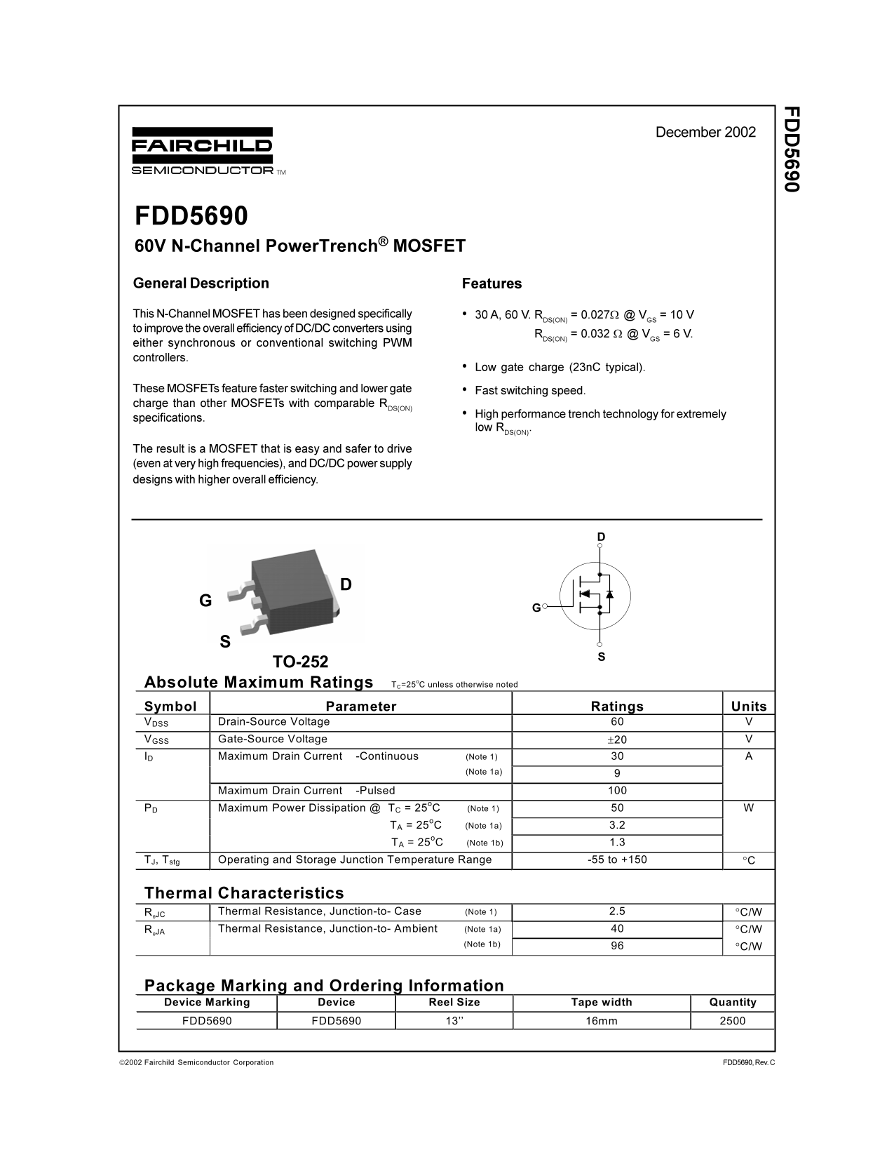
Page 1 Text Content
December 2002
60V N-Channel Power Trench® MOSFET
TO-252
Absolute Maximum Ratings TC=25o C unless otherwise noted Symbol Parameter Ratings Units VDSS Drain-Source Voltage VGSS Gate-Source Voltage ±20 ID Maximum Drain Current -Continuous (Note 1)
(Note 1a)
Maximum Drain Current -Pulsed
PD Maximum Power Dissipation @ TC = 25o C (Note 1)
TA = 25o C (Note 1a) 3.2 TA = 25o C (Note 1b) 1.3
TJ, Tstg Operating and Storage Junction Temperature Range -55 to +150 °C
Thermal Characteristics
RθJC Thermal Resistance, Junction-to- Case (Note 1) 2.5 °C/W RθJA Thermal Resistance, Junction-to- Ambient (Note 1a) °C/W (Note 1b)
Package Marking and Ordering Information Device Marking Device Reel Size Tape width Quantity FDD5690 FDD5690 13’’ 16mm
Page Summary Contents For Fairchild FDD5690 60V N-Channel PowerTrench MOSFET Data Manual
Manual Details
| Brand | Fairchild |
|---|---|
| Pages | 5 |
| File Size | 170.10 KB |
| Published | July 15, 2026 |
Enter the captcha to get the download link:

Frequently Asked Questions
What is the maximum rated drain-source voltage (VDS)?
The absolute maximum rating for Drain-Source Voltage (VDS) is 60 V.
What is the typical on-resistance (Rds(on))?
Under standard test conditions (V=10 V, I=9 A), the typical on-resistance is 0.048 Ω.
How much power can this device safely dissipate?
The maximum power dissipation (@ Tc = 25°C) is 50 W.
What are the turning speed characteristics?
The typical Turn-On Delay Time (t_d(on)) is 16 ns, and the Turn-Off Delay Time (t_d(off)) is 39 ns.