Fairchild FDD5612 60V N-Channel PowerTrench MOSFET Data Sheet
Summary
This powerful N-Channel MOSFET is engineered to maximize efficiency in high-frequency DC/DC converters and advanced power supply designs using PWM controllers. Delivering fast switching capabilities and low gate charge performance, it is ideal for engineers building reliable, high-current switching systems needing optimal energy efficiency. The accompanying datasheet provides a complete resource, detailing crucial electrical specifications, thermal characteristics, and timing parameters necessary for system design integration.
Page 1 Text Content
March 2001
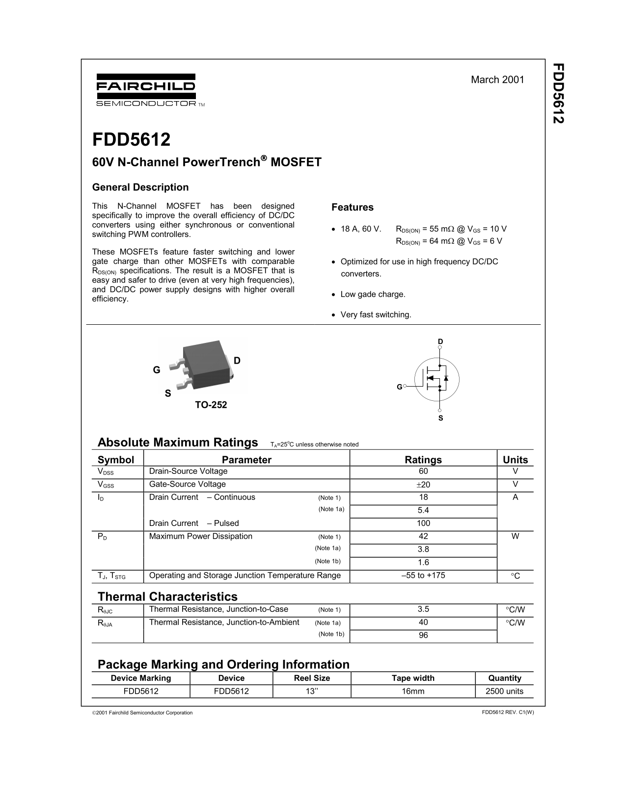
FDD5612 60V N-Channel Power Trench MOSFET General Description This N-Channel MOSFET has been designed Features specifically to improve the overall efficiency of DC/DC converters using either synchronous or conventional
• 18 A, 60 V. RDS(ON) = 55 mΩ @ VGS = 10 V
switching PWM controllers.
RDS(ON) = 64 mΩ @ VGS = 6 V
These MOSFETs feature faster switching and lower gate charge than other MOSFETs with comparable • Optimized for use in high frequency DC/DC RDS(ON) specifications. The result is a MOSFET that is
converters.
easy and safer to drive (even at very high frequencies), and DC/DC power supply designs with higher overall
• Low gade charge.
efficiency.
• Very fast switching.
TO-252
Absolute Maximum Ratings TA=25o C unless otherwise noted Symbol Parameter Ratings Units VDSS Drain-Source Voltage 60 V VGSS Gate-Source Voltage ±20 V ID Drain Current – Continuous (Note 1) 18 A (Note 1a) 5.4 Drain Current – Pulsed 100 PD Maximum Power Dissipation (Note 1) 42
(Note 1a) 3.8 (Note 1b) 1.6
TJ, TSTG Operating and Storage Junction Temperature Range –55 to +175 °C
Thermal Characteristics RθJC Thermal Resistance, Junction-to-Case (Note 1) 3.5 °C/W RθJA Thermal Resistance, Junction-to-Ambient (Note 1a) 40 °C/W (Note 1b) 96
Package Marking and Ordering Information Device Marking Device Reel Size Tape width Quantity FDD5612 FDD5612 13’’ 16mm 2500 units
2001 Fairchild Semiconductor Corporation FDD5612 REV. C1(W)
Page Summary Contents For Fairchild FDD5612 60V N-Channel PowerTrench MOSFET Data Sheet
Manual Details
| Brand | Fairchild |
|---|---|
| Pages | 5 |
| File Size | 80.36 KB |
| Published | July 06, 2026 |
Enter the captcha to get the download link:

Frequently Asked Questions
What applications is this MOSFET optimized for?
It is specifically designed to improve overall efficiency in both synchronous and conventional DC/DC converters.
What are the primary advantages of using this FET?
Advantages include faster switching, lower gate charge, and optimization for high-frequency DC/DC converter designs.
What is the maximum continuous current rating (D)?
The continuous drain current is rated at 18 A. The pulsed rating is up to 100 A.