Fairchild FDD8N50NZ Product Specification Sheet
Summary
The FDD8N50NZ is a robust N-Channel MOSFET designed for high-efficiency power applications, featuring low on-state resistance and superior switching capabilities. This comprehensive manual provides critical technical data, including detailed electrical characteristics, thermal ratings, and performance curves for utilizing this component in demanding environments. Engineered with planar stripe DMOS technology, this device is ideally suited for professionals developing modern switch-mode power supplies (SMPS) and active power factor correction (PFC) circuits requiring reliable, fast, and highly efficient power conversion.
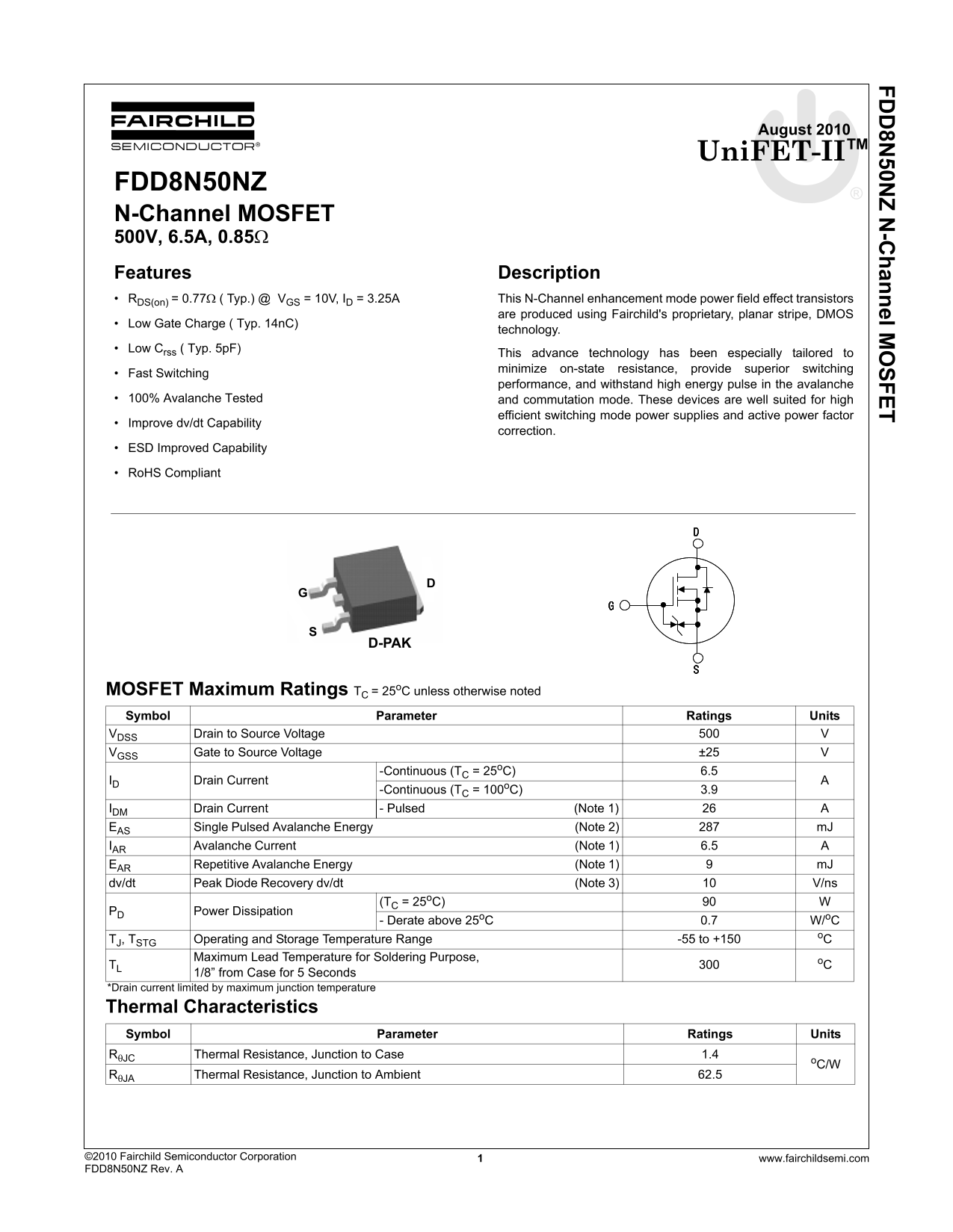
Page 1 Text Content
FD 8N 50N Z N -C hannel M SFET
August 2010
Uni FET-IITM
FDD8N50NZ N-Channel MOSFET 500V, 6.5A, 0.85Ω Features Description RDS(on) = 0.77Ω ( Typ.) @ VGS = 10V, ID = 3.25A This N-Channel enhancement mode power field effect transistors
are produced using Fairchild's proprietary, planar stripe, DMOS
Low Gate Charge ( Typ. 14n C)
technology.
Low Crss ( Typ. 5p F)
This advance technology has been especially tailored to minimize on-state resistance, provide superior switching
Fast Switching
performance, and withstand high energy pulse in the avalanche
100% Avalanche Tested and commutation mode. These devices are well suited for high
efficient switching mode power supplies and active power factor
Improve dv/dt Capability
correction.
ESD Improved Capability
Ro HS Compliant
D-PAK
MOSFET Maximum Ratings TC = 25o C unless otherwise noted Symbol Parameter Ratings Units VDSS Drain to Source Voltage
VGSS Gate to Source Voltage ±25
-Continuous (TC = 25o C) 6.5
ID Drain Current
-Continuous (TC = 100o C) 3.9
IDM Drain Current - Pulsed (Note 1) EAS Single Pulsed Avalanche Energy (Note 2) m J IAR Avalanche Current (Note 1) 6.5 EAR Repetitive Avalanche Energy (Note 1) m J
dv/dt Peak Diode Recovery dv/dt (Note 3) V/ns
(TC = 25o C)
PD Power Dissipation
- Derate above 25o C 0.7 W/o C
TJ, TSTG Operating and Storage Temperature Range -55 to +150 Maximum Lead Temperature for Soldering Purpose, o C
1/8” from Case for 5 Seconds
*Drain current limited by maximum junction temperature
Thermal Characteristics Symbol Parameter Ratings Units
RθJC Thermal Resistance, Junction to Case 1.4
RθJA Thermal Resistance, Junction to Ambient 62.5
©2010 Fairchild Semiconductor Corporation www.fairchildsemi.com1 FDD8N50NZ Rev. A
Page Summary Contents For Fairchild FDD8N50NZ Product Specification Sheet
Manual Details
| Brand | Fairchild |
|---|---|
| Pages | 8 |
| File Size | 638.71 KB |
| Published | July 06, 2026 |
Enter the captcha to get the download link:

Frequently Asked Questions
What are the typical on-state characteristics of this MOSFET?
The static drain to source on resistance (Rds(on)) is typically 0.77 Ω at V=10V and I=3.25A.
How should Power Dissipation be calculated if operating above 25°C?
Power dissipation (Pd) must be derated above 25°C at a rate of 0.7W/°C.
What are the general temperature limits for operation and storage?
The MOSFET operates and stores within a range of -55 to +150 °C.
Does this device support high-energy switching applications?
Yes, it has been avalanche tested and can withstand a single pulsed avalanche energy (EAS) of 287 mJ.