Fairchild FDC653N Specifications
Summary
This high-performance N-channel power FET is engineered for ultra-low resistance, featuring a compact SuperSOT-6 package design ideal for miniaturized electronics. It is specifically designed for applications requiring superior efficiency in battery-powered circuits, including notebook computers, portable phones, and PMIC cards that demand fast switching and minimal in-line power loss. This manual provides comprehensive system details, covering absolute maximum ratings, detailed electrical characteristics (on/off state), dynamic switching performance specifications, and thermal guidelines necessary for reliable high-density circuit integration.
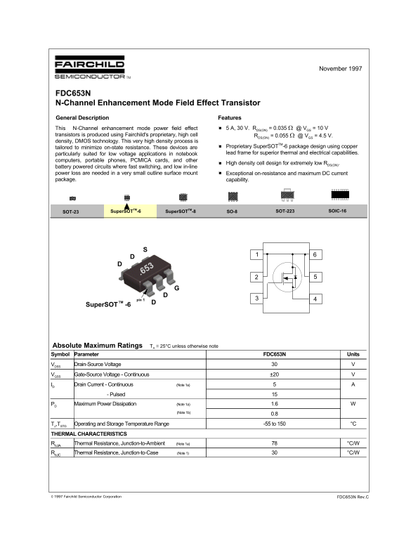
Page 1 Text Content
November 1997
FDC653N N-Channel Enhancement Mode Field Effect Transistor General Description Features
This N-Channel enhancement mode power field effect 5 A, 30 V. RDS(ON) = 0.035 Ω @ VGS = 10 V
transistors is produced using Fairchild's proprietary, high cell RDS(ON) = 0.055 Ω @ VGS = 4.5 V. density, DMOS technology. This very high density process is
tailored to minimize on-state resistance. These devices are Proprietary Super SOTTM-6 package design using copper particularly suited for low voltage applications in notebook lead frame for superior thermal and electrical capabilities.
computers, portable phones, PCMICA cards, and other
High density cell design for extremely low RDS(ON).
battery powered circuits where fast switching, and low in-line power loss are needed in a very small outline surface mount Exceptional on-resistance and maximum DC current package. capability.
Super SOTTM-8 SO-8 SOT-223Super SOTTM-6 SOIC-16SOT-23
Super SOT -6TM
Absolute Maximum Ratings TA = 25°C unless otherwise note Symbol Parameter FDC653N Units
VDSS Drain-Source Voltage
VGSS Gate-Source Voltage - Continuous ±20
ID Drain Current - Continuous (Note 1a)
- Pulsed 15 PD Maximum Power Dissipation (Note 1a) 1.6 (Note 1b)
TJ,TSTG Operating and Storage Temperature Range -55 to 150 °C
THERMAL CHARACTERISTICS RθJA Thermal Resistance, Junction-to-Ambient (Note 1a) °C/W RθJC Thermal Resistance, Junction-to-Case (Note 1) °C/W
© 1997 Fairchild Semiconductor Corporation FDC653N Rev.C
Page Summary Contents For Fairchild FDC653N Specifications
Manual Details
| Brand | Fairchild |
|---|---|
| Pages | 5 |
| File Size | 76.87 KB |
| Published | June 20, 2026 |
Enter the captcha to get the download link:

Frequently Asked Questions
What is the recommended mounting method and thermal resistance?
It requires mounting on a minimum 1 in pad of 2oz Cu in FR-4 board, providing R = 78 °C/W (junction-to-ambient).
What is the maximum drain current capacity?
The continuous drain current can reach up to 5 A. The pulsed rating is higher at 15 Amps.
Is this transistor suitable for portable devices?
Yes, it is particularly suited for low voltage applications in notebook computers and portable phones due to its high density and low on-state resistance.
What is the Gate-Source Voltage (VGS) threshold?
The minimum specified VGS(th) is 1.7V, with a typical value of 2V.