Fairchild FAN5026 Product Specifications
Summary
This high-efficiency Dual DDR/Dual-Output PWM Controller is a robust power management solution designed for sophisticated applications including servers, desktop PCs, and set-top boxes. The device features advanced synchronous switching circuitry and low-loss current sensing, ensuring reliable voltage regulation and optimal performance across memory banks (DDR). This manual provides technical specifications covering operational modes, system integration details, pin definitions, thermal optimization, and comprehensive protection schemes (OVP/UVLO), making it essential for electrical engineers and product designers building reliable, high-power computing systems.
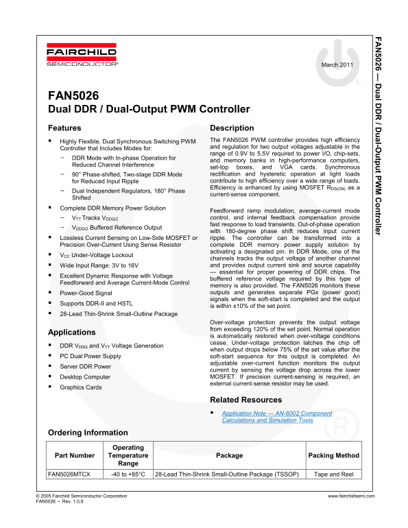
Page 1 Text Content
l D / D l-O tp t P tro lle
March 2011
FAN5026 Dual DDR / Dual-Output PWM Controller Features Description
Highly Flexible, Dual Synchronous Switching PWM The FAN5026 PWM controller provides high efficiency and regulation for two output voltages adjustable in the
Controller that Includes Modes for:
range of 0.9V to 5.5V required to power I/O, chip-sets,
- DDR Mode with In-phase Operation for
and memory banks in high-performance computers,
Reduced Channel Interference
set-top boxes, and VGA cards. Synchronous - 90° Phase-shifted, Two-stage DDR Mode rectification and hysteretic operation at light loads for Reduced Input Ripple contribute to high efficiency over a wide range of loads. Efficiency is enhanced by using MOSFET RDS(ON) as a
- Dual Independent Regulators, 180° Phase
current-sense component.
Shifted
Complete DDR Memory Power Solution
Feedforward ramp modulation, average-current mode - VTT Tracks VDDQ/2 control, and internal feedback compensation provide fast response to load transients. Out-of-phase operation
- VDDQ/2 Buffered Reference Output
with 180-degree phase shift reduces input current
Lossless Current Sensing on Low-Side MOSFET or ripple. The controller can be transformed into a Precision Over-Current Using Sense Resistor complete DDR memory power supply solution by
activating a designated pin. In DDR Mode, one of the
VCC Under-Voltage Lockout
channels tracks the output voltage of another channel Wide Input Range: 3V to 16V and provides output current sink and source capability — essential for proper powering of DDR chips. The
Excellent Dynamic Response with Voltage
buffered reference voltage required by this type of
Feedforward and Average Current-Mode Control
memory is also provided. The FAN5026 monitors these Power-Good Signal outputs and generates separate PGx (power good) signals when the soft-start is completed and the output
Supports DDR-II and HSTL
is within ±10% of the set point.
28-Lead Thin-Shrink Small-Outline Package
Over-voltage protection prevents the output voltage from exceeding 120% of the set point. Normal operation
Applications
is automatically restored when over-voltage conditions cease. Under-voltage protection latches the chip off
DDR VDDQ and VTT Voltage Generation
when output drops below 75% of the set value after the
PC Dual Power Supply soft-start sequence for this output is completed. An
adjustable over-current function monitors the output
Server DDR Power
current by sensing the voltage drop across the lower Desktop Computer MOSFET. If precision current-sensing is required, an external current-sense resistor may be used.
Graphics Cards
Related Resources Application Note — AN-6002 Component Calculations and Simulation Tools
Ordering Information
Operating
Part Number Temperature Package Packing Method
Range
FAN5026MTCX -40 to +85°C 28-Lead Thin-Shrink Small-Outline Package (TSSOP) Tape and Reel
© 2005 Fairchild Semiconductor Corporation www.fairchildsemi.com FAN5026 • Rev. 1.0.8
Page Summary Contents For Fairchild FAN5026 Product Specifications
Manual Details
| Brand | Fairchild |
|---|---|
| Pages | 17 |
| File Size | 752.23 KB |
| Published | June 01, 2026 |
Enter the captcha to get the download link:

Frequently Asked Questions
What input voltage range does the FAN5026 controller support?
The unit supports a wide input range spanning from 3V to 16V.
How does the device handle over-voltage or under-voltage conditions?
It features both over-voltage protection (which restores automatically) and under-voltage protection (which latches the chip off if voltage drops below 75% of the set value).
What is the purpose of DDR Mode operation?
DDR Mode provides high efficiency through advanced techniques like In-phase Operation, 90° Phase-shifted, and Two-stage regulation for memory power solutions.
How can users monitor output current precisely?
For precision current-sensing, an external current-sense resistor may be used to optimize monitoring.