Fairchild MMBFJ202 Product Specifications
Summary
This N-Channel General Purpose Amplifier is designed for robust performance in low-level audio and general electronic applications working with high impedance signal sources. The accompanying manual serves as a comprehensive technical guide for design engineers, detailing operational specifications including absolute maximum ratings, small signal electrical characteristics, thermal management data, and multiple mechanical package options (TO-92/SOT-23). It provides all necessary parameters for reliable circuit development.
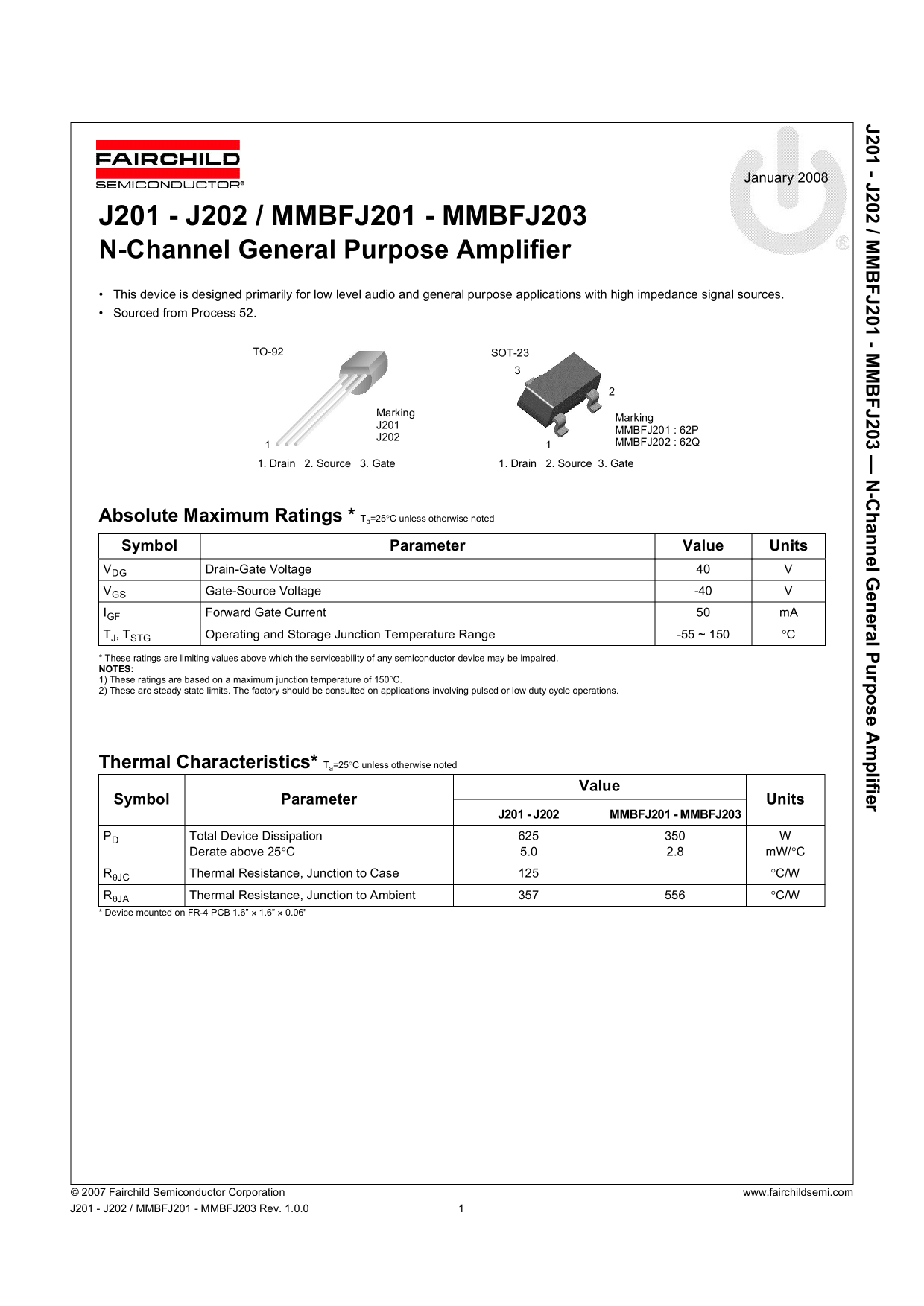
Page 1 Text Content
- J / M - M -C l G ra l P rp lifie
January 2008
J201 - J202 / MMBFJ201 - MMBFJ203 N-Channel General Purpose Amplifier This device is designed primarily for low level audio and general purpose applications with high impedance signal sources. Sourced from Process 52.
SOT-23TO-92
Marking
Marking
MMBFJ201 : 62P
MMBFJ202 : 62Q1
1. Drain 2. Source 3. Gate1. Drain 2. Source 3. Gate
Absolute Maximum Ratings * Ta=25°C unless otherwise noted Symbol Parameter Value Units VDG Drain-Gate Voltage VGS Gate-Source Voltage -40 IGF Forward Gate Current m A TJ, TSTG Operating and Storage Junction Temperature Range -55 ~ 150 °C * These ratings are limiting values above which the serviceability of any semiconductor device may be impaired. NOTES: 1) These ratings are based on a maximum junction temperature of 150°C. 2) These are steady state limits. The factory should be consulted on applications involving pulsed or low duty cycle operations.
Thermal Characteristics* Ta=25°C unless otherwise noted
Value
Symbol Parameter Units
J201 - J202 MMBFJ201 - MMBFJ203
PD Total Device Dissipation
Derate above 25°C 5.0 2.8 m W/°C
Rq JC Thermal Resistance, Junction to Case °C/W
Rq JA Thermal Resistance, Junction to Ambient °C/W * Device mounted on FR-4 PCB 1.6” ´ 1.6” ´ 0.06"
© 2007 Fairchild Semiconductor Corporation www.fairchildsemi.com J201 - J202 / MMBFJ201 - MMBFJ203 Rev. 1.0.0
Page Summary Contents For Fairchild MMBFJ202 Product Specifications
Manual Details
| Brand | Fairchild |
|---|---|
| Pages | 8 |
| File Size | 783.36 KB |
| Published | July 06, 2026 |
Enter the captcha to get the download link:

Frequently Asked Questions
What is the primary intended use of this amplifier?
It is designed primarily for low level audio and general purpose applications with high impedance signal sources.
How should I handle thermal dissipation above 25°C?
Use the derating factor: 5.0 mW/°C (or 2.8 mW/°C depending on required rating).
Are these rated limits for continuous use?
No, these are steady state limits. The factory should be consulted for pulsed or low duty cycle operations.
What kind of voltage breakdown is permitted?
The provided data shows a Drain-Gate Voltage (DG V) maximum rating of 40V and a Gate-Source Voltage (GS) maximum rating of -40V.