# A B C D E F G H I J K L M N O P Q R S T U V W X Y Z

Fairchild Fan5665 Product Specifications

Summary

The FAN5665 is a high-efficiency, adaptive 5V boosted DC/DC converter designed using switched capacitor technology. It reliably steps up voltage for an output range of 2.9V to 5.5V, supporting input voltages from 2.9V to 5.5V and delivering up to 30mA current. The accompanying manual provides comprehensive technical details, covering its built-in protection circuits (UVLO, SCP), low-noise operation, efficiency modes, power pin configuration, and application guidelines. This component is essential for embedded systems designers building portable electronics like cell phones, smart devices, and pocket PCs.
📄 Preview PAGE OF 15

Page 1 Text Content

FA 5665 — igh-Efficiency, A daptive C harge Pum p 5V B oost

February 2008

FAN5665 High-Efficiency, Adaptive Charge Pump 5V Boost

Features Description

5V Fixed Output Voltage The FAN5665 is a 5V switched capacitor step-up DC/DC converter with an input voltage range from 2.9V

30m A Maximum Output Current

to 5.5V. Switch reconfiguration and fractional switching techniques are utilized to achieve high efficiency over

Built-in Charge Pump with Three Modes of

the entire input voltage range.

Operation: 1×, 1.5×, and 2×

Minimum External Components The FAN5665 includes built-in under-voltage lockout, short circuit, and thermal protection circuitry.

Flying Capacitors Only 0.22µF

The FAN5665 is available in an 8-bump 0.4mm pitch

Low-noise, Constant-frequency Operation (1.2MHz)

WLCSP package.

at Heavy Loads High-efficiency, Low-frequency Operation at Light Loads Low Quiescent Current

C1- GND EN

Up to 92% Efficiency

2.9V to 5.5V Input Voltage Range 0.22µF +2.9 to 5.5V

C1+ VIN

Soft-start for Limiting Inrush Current

Input Under-Voltage Lockout Protection (UVLO)

Short-Circuit Protection (SCP) VOUT C2+ C2-

Thermal Shutdown Protection (TSD)

8-bump 1.21 x 1.21mm, 0.4mm Pitch WLCSP C2

Applications USB I/O Supply Regulators

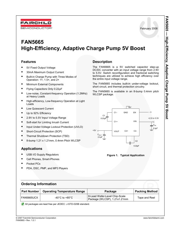
Figure 1. Typical Application

Cell Phones, Smart-Phones Pocket PCs PDA, DSC, PMP, and MP3 Players

Ordering Information

Part Number Operating Temperature Range Package Packing Method

FAN5665UCX -40°C to +85°C 8-Lead Wafer-Level Chip-Scale

Package (WLCSP), 1.21x1.21mm Tape and Reel

All packages are lead free per JEDEC: J-STD-020B standard.

© 2007 Fairchild Semiconductor Corporation www.fairchildsemi.com FAN5665 • Rev. 1.0.1

Page Summary Contents For Fairchild Fan5665 Product Specifications

Page 1 FA 5665 — igh-Efficiency, A daptive C harge Pum p 5V B oost February 2008 FAN5665 High-Efficiency, Adaptive Charge Pump 5V Boost Features Description 5V Fixed Output Voltage The FAN5665 is a 5V switch...
Page 2 FA 5665 — igh-Efficiency, A daptive C harge Pum p 5V B oost Pin Configuration Figure 2. Pin Configuration Pin Definitions Pin # Name Description A1 C1- Bucket capacitor 1. Connect this pin to the nega...
Page 3 FA 5665 — igh-Efficiency, A daptive C harge Pum p 5V B oost Absolute Maximum Ratings Stresses exceeding the absolute maximum ratings may damage the device. The device may not function or be operable a...
Page 4 FA 5665 — igh-Efficiency, A daptive C harge Pum p 5V B oost Electrical Characteristics Unless otherwise noted, VIN = 2.9V to 5.5V, C1 = C2 = 0.22µF, CIN = 2.2µF, COUT = 2.2µF, TA = -40°C to +85°C, and...
Page 5 FA 5665 — igh-Efficiency, A daptive C harge Pum p 5V B oost Typical Performance Characteristics ui es ce nt ur re nt Sw itc hi ng re qu ec (k z) Sw itc hi ng re qu en cy (k z) Unless otherwise noted, ...
Page 6 FA 5665 — igh-Efficiency, A daptive C harge Pum p 5V B oost Typical Performance Characteristics (Continued) Ef fic ie nc ut pu t V ol ta ge (V ut pu t V ol ta ge (V LO hr es ho ld (V Unless otherwise ...
Page 7 FA 5665 — igh-Efficiency, A daptive C harge Pum p 5V B oost Typical Performance Characteristics (Continued) Unless otherwise noted, CIN = 2.2µF, COUT = 2.2µF, C1 = C2 = 0.22µF, TA = 25°C. Figure 17. L...
Page 8 FA 5665 — igh-Efficiency, A daptive C harge Pum p 5V B oost Typical Performance Characteristics (Continued) Unless otherwise noted, CIN = 2.2µF, COUT = 2.2µF, C1 = C2 = 0.22µF, TA = 25°C. Figure 23. L...
Page 9 FA 5665 — igh-Efficiency, A daptive C harge Pum p 5V B oost Typical Performance Characteristics (Continued) Unless otherwise noted, CIN = 2.2µF, COUT = 2.2µF, C1 = C2 = 0.22µF, TA = 25°C. Figure 29. S...
Page 10 FA 5665 — igh-Efficiency, A daptive C harge Pum p 5V B oost Typical Performance Characteristics (Continued) Unless otherwise noted, CIN = 2.2µF, COUT = 2.2µF, C1 = C2 = 0.22µF, TA = 25°C. Figure 35. I...
Page 11 FA 5665 — igh-Efficiency, A daptive C harge Pum p 5V B oost Block Diagram Figure 39. Block Diagram Functional Description Overview Light / Heavy Load Monitor FAN5665 is a 5V switched capacitor regulat...
Page 12 FA 5665 — igh-Efficiency, A daptive C harge Pum p 5V B oost Applications Information The high switching frequency of 1.2MHz allows the use of small capacitors, but the material of the capacitor Bucket...
Page 13 FA 5665 — igh-Efficiency, A daptive C harge Pum p 5V B oost Applications Information (Continued) LED Driver PCB Layout The FAN5665 can be configured as an LED driver, as The PCB layout should be desig...
Page 14 FA 5665 — igh-Efficiency, A daptive C harge Pum p 5V B oost Physical Dimensions Product D E X Y FAN5665UCX 1.210 +/- 0.030mm 1.210 +/- 0.030mm 0.205mm 0.205mm Figure 43. 8-Lead Wafer-Level Chip-Scale ...
Page 15 FA 5665 — igh-Efficiency, A daptive C harge Pum p 5V B oost © 2007 Fairchild Semiconductor Corporation www.fairchildsemi.com FAN5665 • Rev. 1.0.1 15

Manual Details

Brand Fairchild
Pages 15
File Size 709.46 KB
Published May 28, 2026
60 views

Enter the captcha to get the download link:

captcha

Frequently Asked Questions

What is the general operating voltage range for this converter?

The input voltage (VIN) operates from 2.9V to 5.5V, providing a fixed 5V output (VOUT).

What protection features does the FAN5665 include for reliable operation?

It includes built-in under-voltage lockout (UVLO), short circuit (SCP), and thermal shutdown protection (TSD) circuitry.

How much current can this device reliably supply?

The maximum rated output current is 30mA.

Is there a specific package or physical dimension to consider when designing with this IC?

It comes in an 8-bump WLCSP package, measuring 1.21 x 1.21mm.