Fairchild 2N7002W Technical Data Sheet
Summary
This surface-mount N-channel MOSFET is engineered for reliable and high-efficiency power switching applications, featuring low on-resistance and fast switching speed in an SOT-323 package. The comprehensive manual provides designers with all necessary technical specifications. It details absolute maximum ratings, thermal characteristics, input/output capacitance values, and detailed performance curves (including turn-on and turn-off times). This resource is essential for electrical engineers designing circuits requiring stable, compact, and robust solid-state switching components.
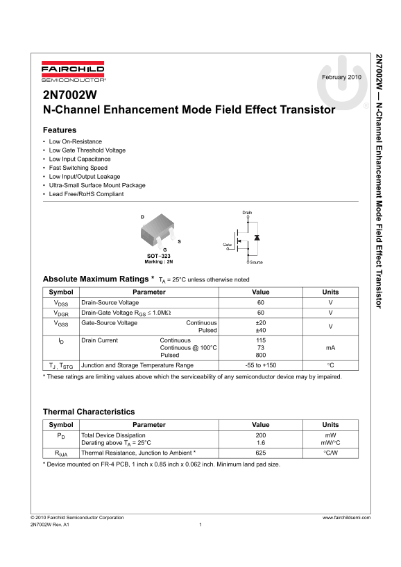
Page 1 Text Content
2N 7002W -C an el E cem en t M e F ield ffect Tran sisto
February 2010
2N7002W N-Channel Enhancement Mode Field Effect Transistor Features Low On-Resistance Low Gate Threshold Voltage Low Input Capacitance Fast Switching Speed Low Input/Output Leakage Ultra-Small Surface Mount Package Lead Free/Ro HS Compliant
SOT-323 Marking : 2N
Absolute Maximum Ratings * TA = 25°C unless otherwise noted Symbol Parameter Value Units VDSS Drain-Source Voltage 60
VDGR Drain-Gate Voltage RGS 1.0M 60 VGSS Gate-Source Voltage Continuous ±20 Pulsed ±40 ID Drain Current Continuous Continuous @ 100°C m A Pulsed TJ , TSTG Junction and Storage Temperature Range -55 to +150 C
* These ratings are limiting values above which the serviceability of any semiconductor device may by impaired.
Thermal Characteristics Symbol Parameter Value Units PD Total Device Dissipation m W
Derating above TA = 25°C 1.6 m W/C RJA Thermal Resistance, Junction to Ambient * 625 C/W
* Device mounted on FR-4 PCB, 1 inch x 0.85 inch x 0.062 inch. Minimum land pad size.
© 2010 Fairchild Semiconductor Corporation www.fairchildsemi.com 2N7002W Rev. A1
Page Summary Contents For Fairchild 2N7002W Technical Data Sheet
Manual Details
| Brand | Fairchild |
|---|---|
| Pages | 6 |
| File Size | 291.43 KB |
| Published | June 18, 2026 |
Enter the captcha to get the download link:
