Toshiba TOSHIBA Field Effect Transistor Silicon P, N Channel MOS Type (U- MOS IV U- MOS III) TPCP8402 Data Manual
Summary
This comprehensive technical manual provides expert specifications for the TPCP8402 N-Channel Power MOSFET transistor. Developed for portable equipment applications, motor drives, and DC-DC converter circuits, this component is crucial for power management in advanced electronics. The guide details maximum ratings, electrical characteristics, thermal performance curves, and handling precautions, providing engineers and hardware designers with all necessary data to ensure safe and optimal circuit implementation.
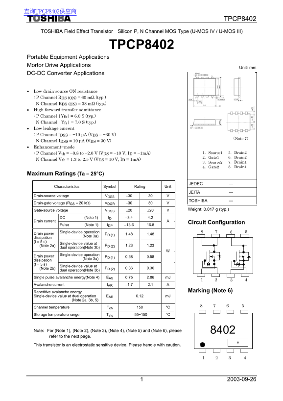
Page 1 Text Content
查询TPCP8402供应商
TPCP8402
TOSHIBA Field Effect Transistor Silicon P, N Channel MOS Type (U-MOS IV / U-MOS III)
TPCP8402
Portable Equipment Applications Mortor Drive Applications
Unit: mm
DC-DC Converter Applications
• Low drain-source ON resistance : P Channel RDS (ON) = 60 mΩ (typ.) N Channel RDS (ON) = 38 mΩ (typ.) • High forward transfer admittance : P Channel |Yfs| = 6.0 S (typ.) N Channel |Yfs| = 7.0 S (typ.) • Low leakage current : P Channel IDSS = −10 µA (VDS = −30 V)
(Note 7)
N Channel IDSS = 10 µA (VDS = 30 V) • Enhancement−mode
: P Channel Vth = −0.8 to −2.0 V (VDS = −10 V, ID = −1m A) 1.Source1 5.Drain2 2.Gate1 6.Drain2
N Channel Vth = 1.3 to 2.5 V (VDS = 10 V, ID = 1m A)
3.Source2 7.Drain1 4.Gate2 8.Drain1
Maximum Ratings (Ta = 25°C)
JEDEC ―
Characteristics Symbol Rating Unit
JEITA ―
Drain-source voltage VDSS −30 30 V
TOSHIBA ―
Drain-gate voltage (RGS = 20 kΩ) VDGR −30 30 V
Gate-source voltage VGSS ±20 ±20 V Weight: 0.017 g (typ.)
DC (Note 1) ID −3.4 4.2
Drain current
Circuit Configuration
Pulse (Note 1) IDP −13.6 16.8 Single-device operation
(Note 3a) PD (1) 1.48 1.48 Drain power
dissipation (t = 5 s) (Note 2a) Single-device value at
dual operation(Note 3b) PD (2) 1.23 1.23 Single-device operation
(Note 3a) PD (1) 0.58 0.58 Drain power
dissipation (t = 5 s) (Note 2b) Single-device value at
dual operation(Note 3b) PD (2) 0.36 0.36
Single pulse avalanche energy(Note 4) EAS 0.75 2.86 m J Avalanche current IAR −1.7 2.1 A
Repetitive avalanche energy Marking (Note 6)
Single-device value at dual operation EAR 0.12 m J (Note 2a, 3b, 5)
Channel temperature Tch 150 °C Storage temperature range Tstg −55~150 °C
Note: For (Note 1), (Note 2), (Note 3), (Note 4), (Note 5) and (Note 6), please refer to the next page.
This transistor is an electrostatic sensitive device. Please handle with caution.
Page Summary Contents For Toshiba TOSHIBA Field Effect Transistor Silicon P, N Channel MOS Type (U- MOS IV U- MOS III) TPCP8402 Data Manual
Manual Details
| Brand | Toshiba |
|---|---|
| Pages | 6 |
| File Size | 158.40 KB |
| Published | June 05, 2026 |
Enter the captcha to get the download link:

Frequently Asked Questions
What precautions should be taken when handling this component?
The transistor is considered an electrostatic sensitive device and must be handled with caution.
Can I use these components in life-critical systems like medical equipment?
No. The product is not warranted for ‘Unintended Usage,’ such as medical instruments or airplane instruments, which require extraordinarily high reliability.
What are the required operating conditions before maximum usage?
You must ensure that the channel temperature remains below 150°C when developing designs.
Which mounting materials are compatible with this device?
It is designed for use on glass-epoxy boards or FR-4 material.