Texas Instruments TC211 Data Manual
Summary
This full-frame CCD image sensor is engineered for demanding industrial applications requiring reliability and small form factor imaging. Featuring 192x165 pixels, it includes advanced features like antiblooming capability and high photoresponse uniformity. The accompanying manual provides comprehensive technical details on its operation—from charge collection to signal processing—and essential guidelines for handling this robust, 6-pin dual-in-line ceramic package. Ideal for engineers designing specialized industrial imaging systems.
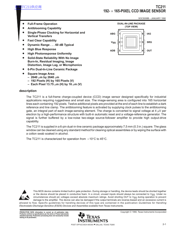
Page 1 Text Content
查询TC211供应商 TC211
192- 165-PIXEL CCD IMAGE SENSOR
SOCS008B – JANUARY 1990
Full-Frame Operation DUAL-IN-LINE PACKAGE (TOP VIEW)
Antiblooming Capability Single-Phase Clocking for Horizontal and
ABG IAG
Vertical Transfers Fast Clear Capability
VSS SRG
Dynamic Range 60 d B Typical High Blue Response
ADB OUT
High Photoresponse Uniformity Solid-State Reliability With No Image Burn-In, Residual Imaging, Image Distortion, Image Lag, or Microphonics 6-Pin Dual-In-Line Ceramic Package Square Image Area: – 2640 µm by 2640 µm – 192 Pixels (H) by 165 Pixels (V) – Each Pixel 13.75 µm (H) by 16 µm (V)
description The TC211 is a full-frame charge-coupled device (CCD) image sensor designed specifically for industrial applications requiring ruggedness and small size. The image-sensing area is configured into 165 horizontal lines each containing 192 pixels. Twelve additional pixels are provided at the end of each line to establish a dark reference and line clamp. The antiblooming feature is activated by supplying clock pulses to the antiblooming gate, an integral part of each image-sensing element. The charge is converted to signal voltage at 4 µV per electron by a high-performance structure with built-in automatic reset and a voltage-reference generator. The signal is further buffered by a low-noise two-stage source-follower amplifier to provide high output-drive capability. The TC211 is supplied in a 6-pin dual-in-line ceramic package approximately 7,5 mm (0.3 in.) square. The glass window can be cleaned using any standard method for cleaning optical assemblies or by wiping the surface with a cotton swab soaked in alcohol. The TC211 is characterized for operation from –10°C to 45°C.
This MOS device contains limited built-in gate protection. During storage or handling, the device leads should be shorted together or the device should be placed in conductive foam. In a circuit, unused inputs should always be connected to VSS. Under no circumstances should pin voltages exceed absolute maximum ratings. Avoid shorting OUT to VSS during operation to prevent damage to the amplifier. The device can also be damaged if the output terminals are reverse-biased and an excessive current is
allowed to flow. Specific guidelines for handling devices of this type are contained in the publication Guidelines for Handling Electrostatic-Discharge-Sensitive (ESDS) Devices and Assemblies available from Texas Instruments.
PRODUCTION DATA information is current as of publication date. Copyright 1990, Texas Instruments Incorporated
Products conform to specifications per the terms of Texas Instruments standard warranty. Production processing does not necessarily include testing of all parameters.
2-1POST OFFICE BOX 655303 • DALLAS, TEXAS 75265
Page Summary Contents For Texas Instruments TC211 Data Manual
Manual Details
| Brand | Texas Instruments |
|---|---|
| Pages | 13 |
| File Size | 176.36 KB |
| Published | June 18, 2026 |
Enter the captcha to get the download link:

Frequently Asked Questions
How should I store or handle the sensor device?
During storage or handling, the device leads must be shorted together or placed in conductive foam.
What materials can I use to clean the glass window?
You can use any standard method for cleaning optical assemblies or wipe it with a cotton swab soaked in alcohol.
How does the dark reference function improve image quality?
The 12 dark pixels generate a dark reference signal, which is used to restore and maintain the video black level on subsequent image lines.
What common electrical mistake should I avoid when operating the device?
Do not short OUT to V during operation to prevent damage to the amplifier, and check that pin voltages do not exceed absolute maximum ratings.