Texas Instruments SN74AVCH245 Data Sheet / Manual
Summary
This datasheet provides comprehensive details on the SN74AVCH245, a high-performance octal bus transceiver designed for robust asynchronous data communication in mixed-voltage environments. Featuring Dynamic Output Control (DOC) and EPIC technology, this component assures superior noise reduction and excellent signal integrity across multiple power levels (1.2V to 3.6V). The manual covers the operational principles, functional tables, pin assignments, and specialized use cases for engineers requiring reliable data transfer modules, including those utilizing partial-power-down modes.
Page 1 Text Content
SN74AVCH245
OCTAL BUS TRANSCEIVER WITH 3-STATE OUTPUTS SCES264D – APRIL 1999 – REVISED FEBRUARY 2000
DOC (Dynamic Output Control) Circuit Overvoltage-Tolerant Inputs/Outputs Allow tp Vo lt ag Dynamically Changes Output Impedance, Mixed-Voltage-Mode Data Communications Resulting in Noise Reduction Without
Ioff Supports Partial-Power-Down Mode
Speed Degradation
Operation
EPIC (Enhanced-Performance Implanted
Bus Hold on Data Inputs Eliminates the
CMOS) Submicron Process
Need for External Pullup/Pulldown Less Than 2-ns Maximum Propagation Resistors
Delay at 2.5-V and 3.3-V VCC
Package Options Include Plastic
Dynamic Drive Capability Is Equivalent to Small-Outline (DW), Thin Very
Standard Outputs With IOH and IOL of Small-Outline (DGV), and Thin Shrink ±24 m A at 2.5-V VCC Small-Outline (PW) Packages
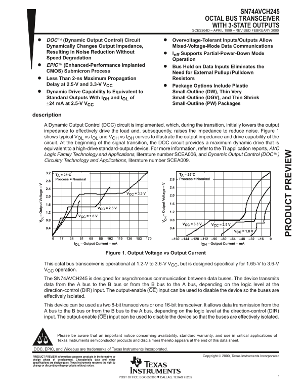
description A Dynamic Output Control (DOC) circuit is implemented, which, during the transition, initially lowers the output impedance to effectively drive the load and, subsequently, raises the impedance to reduce noise. Figure 1 shows typical VOL vs IOL and VOH vs IOH curves to illustrate the output impedance and drive capability of the circuit. At the beginning of the signal transition, the DOC circuit provides a maximum dynamic drive that is equivalent to a high-drive standard-output device. For more information, refer to the TI application reports, AVC Logic Family Technology and Applications, literature number SCEA006, and Dynamic Output Control (DOC) Circuitry Technology and Applications, literature number SCEA009.
tp Vo lt ag
TA = 25°C TA = 25°C Process = Nominal 2.8 Process = Nominal
VCC = 3.3 V
VCC = 2.5 V
VCC = 1.8 V–
0.8 0.8 VCC = 3.3 V VCC = 2.5 V 0.4 0.4
VCC = 1.8 V
–128–144–160 –80–96–112 –32–48–64 0–16 IOL – Output Current – m A IOH – Output Current – m A
Figure 1. Output Voltage vs Output Current
This octal bus transceiver is operational at 1.2-V to 3.6-V VCC, but is designed specifically for 1.65-V to 3.6-V VCC operation. The SN74AVCH245 is designed for asynchronous communication between data buses. The device transmits data from the A bus to the B bus or from the B bus to the A bus, depending on the logic level at the
direction-control (DIR) input. The output-enable (OE) input can be used to disable the device so the buses are IE
effectively isolated. This device can be used as two 8-bit transceivers or one 16-bit transceiver. It allows data transmission from the A bus to the B bus or from the B bus to the A bus, depending on the logic level at the direction-control (DIR) input. The output-enable (OE) input can be used to disable the device so that the buses are effectively isolated.
Please be aware that an important notice concerning availability, standard warranty, and use in critical applications of Texas Instruments semiconductor products and disclaimers thereto appears at the end of this data sheet.
DOC, EPIC, and Widebus are trademarks of Texas Instruments Incorporated.
PRODUCT PREVIEW information concerns products in the formative or Copyright 2000, Texas Instruments Incorporated
design phase of development. Characteristic data and other specifications are design goals. Texas Instruments reserves the right to change or discontinue these products without notice.
1POST OFFICE BOX 655303 • DALLAS, TEXAS 75265
Page Summary Contents For Texas Instruments SN74AVCH245 Data Sheet / Manual
Manual Details
| Brand | Texas Instruments |
|---|---|
| Pages | 12 |
| File Size | 176.25 KB |
| Published | June 02, 2026 |
Enter the captcha to get the download link:

Frequently Asked Questions
What is the operating temperature range for this device?
The SN74AVCH245 is characterized for operation from -40°C to 85°C.
How can I ensure bus isolation when turning the device off?
Use the output-enable (OE) input. If powering down, OE should be tied to V through a pullup resistor.
Does this chip support multiple transceiving functions?
Yes, it can function as two 8-bit transceivers or one single 16-bit transceiver.
What mechanism reduces noise during data transmission?
The Dynamic Output Control (DOC) circuit lowers and subsequently raises the output impedance during signal transitions to reduce noise.