Texas Instruments SN54ABT16543, SN74ABT16543 - 16-BIT REGISTERED TRANCEIVERS WITH 3-STATE OUTPUTS Technical Manual Data Sheet User Guide
Summary
These high-performance 16-bit registered transceivers provide robust, bidirectional data transfer pathways essential for advanced digital systems. The associated manual offers comprehensive technical specifications, detailing operating modes, flow control protocols, and optimized architecture suitable for minimizing high-speed switching noise. Ideal for electrical engineers and hardware designers creating complex electronic interfaces that demand reliable signal integrity across diverse applications.
Page 1 Text Content
查询5962-9324101MXA供应商 SN54ABT16543, SN74ABT16543
16-BIT REGISTERED TRANSCEIVERS
WITH 3-STATE OUTPUTS SCBS087C – FEBRUARY 1991 – REVISED JANUARY 1997
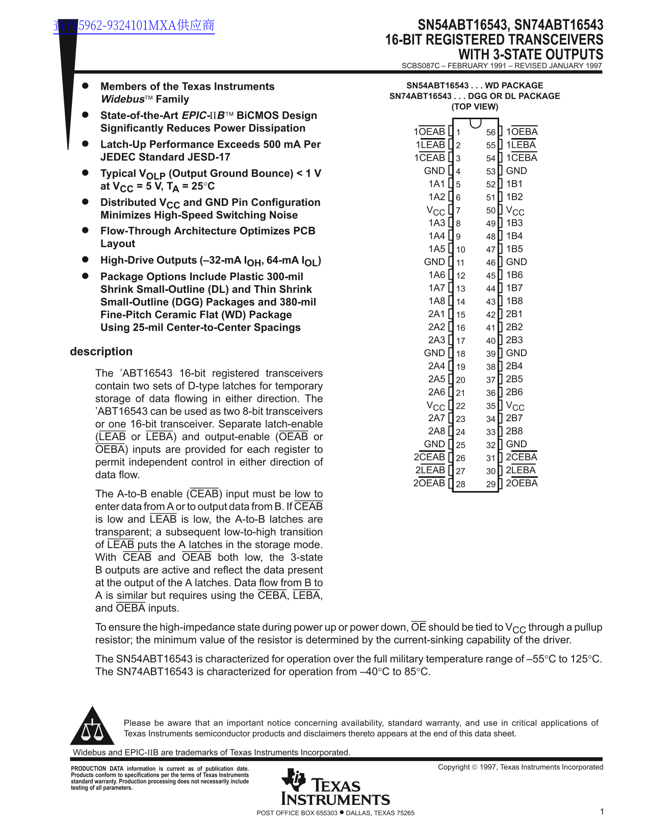
Members of the Texas Instruments SN54ABT16543 WD PACKAGE SN74ABT16543 DGG OR DL PACKAGE
Widebus Family
(TOP VIEW)
State-of-the-Art EPIC-ΙΙB Bi CMOS Design Significantly Reduces Power Dissipation
1OEAB 1OEBA
Latch-Up Performance Exceeds 500 m A Per 1LEAB 1LEBA JEDEC Standard JESD-17 1CEAB 1CEBA
GND GND
Typical VOLP (Output Ground Bounce) < 1 V
at VCC = 5 V, TA = 25°C 1A1 1B1 1A2 1B2
Distributed VCC and GND Pin Configuration
VCC VCC
Minimizes High-Speed Switching Noise
Flow-Through Architecture Optimizes PCB
Layout
High-Drive Outputs (–32-m A IOH, 64-m A IOL) GND GND
Package Options Include Plastic 300-mil 1A6 1B6 Shrink Small-Outline (DL) and Thin Shrink 1A7 1B7 Small-Outline (DGG) Packages and 380-mil 1A8 1B8 Fine-Pitch Ceramic Flat (WD) Package 2A1 2B1 Using 25-mil Center-to-Center Spacings 2A2 2B2 2A3 2B3
description GND GND
The ’ABT16543 16-bit registered transceivers
contain two sets of D-type latches for temporary
storage of data flowing in either direction. The
VCC VCC
’ABT16543 can be used as two 8-bit transceivers
or one 16-bit transceiver. Separate latch-enable
(LEAB or LEBA) and output-enable (OEAB or
GND GND
OEBA) inputs are provided for each register to
2CEAB 2CEBA
permit independent control in either direction of
2LEAB 2LEBA
data flow.
2OEAB 2OEBA
The A-to-B enable (CEAB) input must be low to enter data from A or to output data from B. If CEAB is low and LEAB is low, the A-to-B latches are transparent; a subsequent low-to-high transition of LEAB puts the A latches in the storage mode. With CEAB and OEAB both low, the 3-state B outputs are active and reflect the data present at the output of the A latches. Data flow from B to A is similar but requires using the CEBA, LEBA, and OEBA inputs. To ensure the high-impedance state during power up or power down, OE should be tied to VCC through a pullup resistor; the minimum value of the resistor is determined by the current-sinking capability of the driver. The SN54ABT16543 is characterized for operation over the full military temperature range of –55°C to 125°C. The SN74ABT16543 is characterized for operation from –40°C to 85°C.
Please be aware that an important notice concerning availability, standard warranty, and use in critical applications of Texas Instruments semiconductor products and disclaimers thereto appears at the end of this data sheet.
Widebus and EPIC-ΙΙB are trademarks of Texas Instruments Incorporated.
Copyright 1997, Texas Instruments Incorporated PRODUCTION DATA information is current as of publication date.
Products conform to specifications per the terms of Texas Instruments standard warranty. Production processing does not necessarily include testing of all parameters.
1POST OFFICE BOX 655303 • DALLAS, TEXAS 75265
Page Summary Contents For Texas Instruments SN54ABT16543, SN74ABT16543 - 16-BIT REGISTERED TRANCEIVERS WITH 3-STATE OUTPUTS Technical Manual Data Sheet User Guide
Manual Details
| Brand | Texas Instruments |
|---|---|
| Pages | 13 |
| File Size | 201.08 KB |
| Published | July 15, 2026 |
Enter the captcha to get the download link:

Frequently Asked Questions
How can I configure the ABT16543 chip?
The device can function as two independent 8-bit transceivers or be utilized as one integrated 16-bit transceiver.
What is required for proper power management with the Output Enable (OE) input?
To ensure the high-impedance state during power up or power down, OE must be tied to V through a pullup resistor.
What are the temperature ranges for the two variants?
The SN54ABT16543 is specified for –55°C to 125°C, while the SN74ABT16543 operates from –40°C to 85°C.
What process minimizes noise during high-speed switching?
The internal pin configuration and careful design minimize high-speed switching noise, keeping typical V (Output Ground Bounce) below 1V.