Texas Instruments SN74AUC2G125 Dual Bus Buffer Gate with 3-State Outputs - Data Sheet, Owner's Manual & User Guide
Summary
This advanced dual bus buffer gate provides reliable signal buffering with low power consumption, optimized for modern 1.65V to 1.95V digital systems. Featuring 3-state outputs and supporting mixed-mode operation, it excels in partial power-down applications within space-constrained NanoStar or NanoFree packages. This manual details the electrical specifications, package options, and operational guidelines necessary for engineers designing high-performance, low-voltage integrated circuit logic.
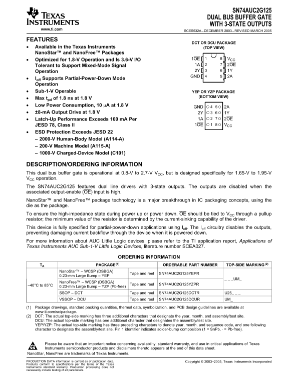
Page 1 Text Content
SN74AUC2G125
DUAL BUS BUFFER GATE
WITH 3-STATE OUTPUTS
www.ti.com
SCES532A–DECEMBER 2003–REVISED MARCH
FEATURES
DCT OR DCU PACKAGE
Available in the Texas Instruments (TOP VIEW)
Nano Star™ and Nano Free™ Packages
1OE VCC
Optimized for 1.8-V Operation and Is 3.6-V I/O
1A 2OE
Tolerant to Support Mixed-Mode Signal
Operation 2Y 1Y
GND 2A
Ioff Supports Partial-Power-Down Mode
Operation
Sub-1-V Operable YEP OR YZP PACKAGE
(BOTTOM VIEW)
Max tpd of 1.8 ns at 1.8
Low Power Consumption, µA at 1.8
GND 2A
±8-m A Output Drive at 1.8 2Y 1Y
Latch-Up Performance Exceeds m A Per 1A 2OE
JESD 78, Class II 1OE VCC
ESD Protection Exceeds JESD
2000-V Human-Body Model (A114-A)
200-V Machine Model (A115-A)
1000-V Charged-Device Model (C101)
DESCRIPTION/ORDERING INFORMATION
This dual bus buffer gate is operational at 0.8-V to 2.7-V VCC, but is designed specifically for 1.65-V to 1.95-V
VCC operation.
The SN74AUC2G125 features dual line drivers with 3-state outputs. The outputs are disabled when the
associated output-enable (OE) input is high.
Nano Star™ and Nano Free™ package technology is major breakthrough in IC packaging concepts, using the
die as the package.
To ensure the high-impedance state during power up or power down, OE should be tied to VCC through pullup
resistor; the minimum value of the resistor is determined by the current-sinking capability of the driver.
This device is fully specified for partial-power-down applications using Ioff. The Ioff circuitry disables the outputs,
preventing damaging current backflow through the device when it is powered down.
For more information about AUC Little Logic devices, please refer to the TI application report, Applications of
Texas Instruments AUC Sub-1-V Little Logic Devices, literature number SCEA027.
ORDERING INFORMATION
TA PACKAGE ORDERABLE PART NUMBER TOP-SIDE MARKING
Nano Star™ WCSP (DSBGA)
Tape and reel SN74AUC2G125YEPR0.23-mm
Large Bump YEP
Nano Free™ WCSP (DSBGA)
Tape and reel SN74AUC2G125YZPR–40°C
to 85°C
0.23-mm Large Bump YZP (Pb-free)
SSOP DCT Tape and reel SN74AUC2G125DCTR U25_
VSSOP DCU Tape and reel SN74AUC2G125DCUR UM_
(1) Package drawings, standard packing quantities, thermal data, symbolization, and PCB design guidelines are available at
www.ti.com/sc/package.
(2) DCT: The actual top-side marking has three additional characters that designate the year, month, and assembly/test site.
DCU: The actual top-side marking has one additional character that designates the assembly/test site.
YEP/YZP: The actual top-side marking has three preceding characters to denote year, month, and sequence code, and one following
character to designate the assembly/test site. Pin identifier indicates solder-bump composition (1 Sn Pb, Pb-free).
Please be aware that an important notice concerning availability, standard warranty, and use in critical applications of Texas
Instruments semiconductor products and disclaimers thereto appears at the end of this data sheet.
Nano Star, Nano Free are trademarks of Texas Instruments.
PRODUCTION DATA information is current as of publication date. Copyright 2003–2005, Texas Instruments Incorporated
Products conform to specifications per the terms of the Texas
Instruments standard warranty. Production processing does not
necessarily include testing of all parameters.
Page Summary Contents For Texas Instruments SN74AUC2G125 Dual Bus Buffer Gate with 3-State Outputs - Data Sheet, Owner's Manual & User Guide
Manual Details
| Brand | Texas Instruments |
|---|---|
| Pages | 12 |
| File Size | 263.90 KB |
| Published | June 06, 2026 |
Enter the captcha to get the download link:

Frequently Asked Questions
What is the optimal operating voltage range for this buffer gate?
While operational at 0.8-V to 2.7-V CC V, it is specifically designed for 1.65-V to 1.95-V CC V operation.
How does the device prevent damaging current backflow during power-down?
The internal circuitry (I) disables the outputs, thereby preventing damaging current backflow when the device is powered down.
What are the key features of the NanoStar™ and NanoFree™ packages?
These package technologies use the die itself as the package, enhancing performance while maintaining reliable high-impedance states for OE.
Is a pullup resistor required to operate in the high-impedance state?
Yes, for OE to ensure the device is in a high-impedance state during power up or power down, it should be tied to V through a pullup CC resistor.