Texas Instruments CD74AC14 Specifications and User's Manual
Summary
The CD74AC14 is a high-precision logic IC designed for signal inversion and buffering, featuring six independent inverters with robust Schmitt trigger action for clean digital signaling. This technical manual provides comprehensive documentation, including electrical characteristics, absolute maximum ratings, packaging options (PDIP, SOIC), and detailed guidelines required for seamless circuit integration. It is essential reading for hardware engineers and electronic designers developing reliable digital systems that require stable logic buffering and high electrostatic discharge (ESD) protection across challenging operating conditions.
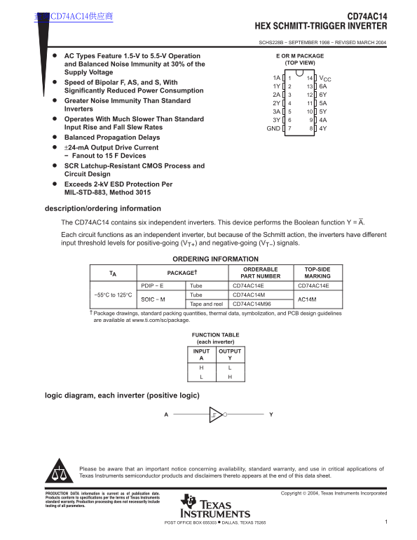
Page 1 Text Content
查询CD74AC14供应商
SCHS228B − SEPTEMBER 1998 − REVISED MARCH 2004
AC Types Feature 1.5-V to 5.5-V Operation E OR M PACKAGE and Balanced Noise Immunity at 30% of the (TOP VIEW)
Supply Voltage
1A VCC
Speed of Bipolar F, AS, and S, With
Significantly Reduced Power Consumption
Greater Noise Immunity Than Standard
Inverters
Operates With Much Slower Than Standard 3Y 4A Input Rise and Fall Slew Rates GND 4Y Balanced Propagation Delays ±24-m A Output Drive Current − Fanout to 15 F Devices SCR Latchup-Resistant CMOS Process and Circuit Design Exceeds 2-k V ESD Protection Per MIL-STD-883, Method 3015
description/ordering information The CD74AC14 contains six independent inverters. This device performs the Boolean function Y = A. Each circuit functions as an independent inverter, but because of the Schmitt action, the inverters have different input threshold levels for positive-going (VT+) and negative-going (VT−) signals.
ORDERING INFORMATION
ORDERABLE TOP-SIDE
TA PACKAGE†
PART NUMBER MARKING
PDIP − E Tube CD74AC14E CD74AC14E
−55°C to 125°C Tube CD74AC14M
SOIC − M AC14M
Tape and reel CD74AC14M96
Package drawings, standard packing quantities, thermal data, symbolization, and PCB design guidelines are available at www.ti.com/sc/package.
FUNCTION TABLE (each inverter) INPUT OUTPUT
logic diagram, each inverter (positive logic)
Please be aware that an important notice concerning availability, standard warranty, and use in critical applications of Texas Instruments semiconductor products and disclaimers thereto appears at the end of this data sheet.
1POST OFFICE BOX 655303 • DALLAS, TEXAS 75265
Page Summary Contents For Texas Instruments CD74AC14 Specifications and User's Manual
Manual Details
| Brand | Texas Instruments |
|---|---|
| Pages | 8 |
| File Size | 242.64 KB |
| Published | May 31, 2026 |
Enter the captcha to get the download link:

Frequently Asked Questions
How does this device differentiate between rising and falling edges?
It utilizes Schmitt action, which provides different input threshold levels for positive-going (V+) and negative-going (V-) signals.
What is the operational supply voltage range for the CD74AC14?
The recommended operating supply voltage range is between 1.5 V and 5.5 V.
Are there specific rules for unused inputs?
Yes, all unused inputs of the device must be held at V or GND to ensure proper operation.
What level of protection does this component offer?
The CD74AC14 exceeds 2-kV ESD protection and uses a latchup-resistant CMOS process design.