# A B C D E F G H I J K L M N O P Q R S T U V W X Y Z

Texas Instruments TPS2014 TPS2015 User's Manual and Specifications

Summary

The TPS20xx is a highly reliable, high-side power MOSFET switch designed for robust load management in applications susceptible to short circuits or heavy capacitive loads. This technical guide details the device's full functionality, covering integrated protection features such as thermal cutoff, undervoltage lockout (UVLO), and precise overcurrent limiting. It provides essential specifications and operational data needed by electrical engineers designing durable power distribution systems with minimal electromagnetic interference (EMI).
📄 Preview PAGE OF 23

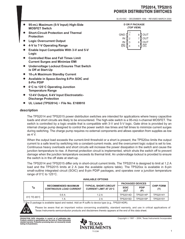
Page 1 Text Content

SLVS159C − DECEMBER 1996 − REVISED MARCH 2004

95-mΩ Maximum (5-V Input) High-Side D OR P PACKAGE (TOP VIEW)

MOSFET Switch Short-Circuit Protection and Thermal

GND OUT

Protection

IN OUT

Logic Overcurrent Output

IN OUT

4-V to 7-V Operating Range EN OC Enable Input Compatible With 3-V and 5-V Logic Controlled Rise and Fall Times Limit Current Surges and Minimize EMI Undervoltage Lockout Ensures That Switch is Off at Start-Up 10-µA Maximum Standby Current Available in Space-Saving 8-Pin SOIC and 8-Pin PDIP 0°C to 125°C Operating Junction Temperature Range 12-k V Output, 6-k V Input Electrostatic- Discharge Protection UL Listed (TPS2014) − File No. E169910

description The TPS2014 and TPS2015 power distribution switches are intended for applications where heavy capacitive loads and short circuits are likely to be encountered. The high-side switch is a 95-mΩ n-channel MOSFET. The switch is controlled by a logic enable that is compatible with 3-V and 5-V logic. Gate drive is provided by an internal charge pump designed to control the power switch rise times and fall times to minimize current surges during switching. The charge pump requires no external components and allows operation from supplies as low as 4 V. When the output load exceeds the current-limit threshold or a short is present, the TPS20xx limits the output current to a safe level by switching into a constant-current mode, and the overcurrent logic output is set to low. Continuous heavy overloads and short circuits will increase the power dissipation in the switch and cause the junction temperature to rise. A thermal protection circuit is implemented, which shuts the switch off to prevent damage when the junction temperature exceeds its thermal limit. An undervoltage lockout is provided to ensure the switch is in the off state at start-up. The TPS2014 and TPS2015 differ only in short-circuit current limits. The TPS2014 is designed to limit at 1.2 load and the TPS2015 limits at 2 A (see the available options table). The TPS20xx is available in 8-pin small-outline integrated circuit (SOIC) and 8-pin PDIP packages, and operates over a junction temperature range of 0°C to 125°C.

AVAILABLE OPTIONS

PACKAGED DEVICES

RECOMMENDED MAXIMUM TYPICAL SHORT-CIRCUIT CHIP FORM

TA SOIC PDIP

CONTINUOUS LOAD CURRENT CURRENT LIMIT AT 25°C (Y)

0.6 A 1.2 A TPS2014D TPS2014P TPS2014Y

0°C TO 85°C

1 A 2 A TPS2015D TPS2015P TPS2015Y

The D package is available taped and reeled. Add an R suffix to device type (e.g., TPS2014DR).

Please be aware that an important notice concerning availability, standard warranty, and use in critical applications of Texas Instruments semiconductor products and disclaimers thereto appears at the end of this data sheet.

1TI.COM

Page Summary Contents For Texas Instruments TPS2014 TPS2015 User's Manual and Specifications

Page 1 SLVS159C − DECEMBER 1996 − REVISED MARCH 2004 95-mΩ Maximum (5-V Input) High-Side D OR P PACKAGE (TOP VIEW) MOSFET Switch Short-Circuit Protection and Thermal GND OUT Protection IN OUT Logic Overcurre...
Page 2 SLVS159C − DECEMBER 1996 − REVISED MARCH 2004 functional block diagram Power Switch IN CS OUT Charge Pump Current EN Driver Limit Thermal GND Sense †Current Sense TPS20xx Y chip information This chip,...
Page 3 SLVS159C − DECEMBER 1996 − REVISED MARCH 2004 Terminal Functions TERMINAL I/O DESCRIPTION NAME NO. EN Enable input. Logic low at EN turns the power switch on. GND Ground IN 2, 3 Input voltage OC OC is...
Page 4 SLVS159C − DECEMBER 1996 − REVISED MARCH 2004 absolute maximum ratings over operating free-air temperature range (unless otherwise noted)† Input voltage range, VI (see Note1) −0.3 V to 7 V. . . . . . ...
Page 5 SLVS159C − DECEMBER 1996 − REVISED MARCH 2004 electrical characteristics over recommended operating junction temperature range, VI(IN)= 5.5 V, IO = rated current, EN = 0 V (unless otherwise noted) (co...
Page 6 SLVS159C − DECEMBER 1996 − REVISED MARCH 2004 electrical characteristics over recommended operating junction temperature range, VI(IN)= 5.5 V, IO = rated current, EN = 0 V (unless otherwise noted) pow...
Page 7 SLVS159C − DECEMBER 1996 − REVISED MARCH 2004 electrical characteristics over recommended operating junction temperature range, VI(IN)= 5.5 V, IO = rated current, EN = 0 V (unless otherwise noted) (co...
Page 8 SLVS159C − DECEMBER 1996 − REVISED MARCH 2004 PARAMETER MEASUREMENT INFORMATION tp Vo lt ag ab le lt ag t − Time − ms Figure 2. Propagation Delay and Fall Time With 1-µF Load, VI(IN) = 5 V tp Vo lt ag...
Page 9 SLVS159C − DECEMBER 1996 − REVISED MARCH 2004 PARAMETER MEASUREMENT INFORMATION −10 tp Vo lt ag tp Vo lt ag t − Time − ms Figure 4. TPS2015 Short-Circuit Current. Short is Applied to Enabled Device, V...
Page 10 SLVS159C − DECEMBER 1996 − REVISED MARCH 2004 PARAMETER MEASUREMENT INFORMATION tp rr en tp Vo lt ag t − Time − ms Figure 6. TPS2015 Threshold Current, VI(IN) = 5 V tp rr en t − Time − ms Figure 7. TP...
Page 11 SLVS159C − DECEMBER 1996 − REVISED MARCH 2004 PARAMETER MEASUREMENT INFORMATION tp rr en t − Time − ms Figure 8. TPS2015 (Enabled) into Short Circuit, VI(IN) = 5 V TYPICAL CHARACTERISTICS Table of Gra...
Page 12 is Ti Tu rn -O el ay im SLVS159C − DECEMBER 1996 − REVISED MARCH 2004 TYPICAL CHARACTERISTICS TURN-ON DELAY TIME TURN-OFF DELAY TIME vs vs INPUT VOLTAGE INPUT VOLTAGE TJ = 25°C TJ = 25°C CL = 1 µF CL ...
Page 13 SLVS159C − DECEMBER 1996 − REVISED MARCH 2004 ly rr en t, tp ab le (O ly rr en t, tp ab le TYPICAL CHARACTERISTICS SUPPLY CURRENT, OUTPUT ENABLED SUPPLY CURRENT, OUTPUT DISABLED vs vs JUNCTION TEMPERA...
Page 14 -S ta te es is ta ce to In Vo lt ag to tp Vo lt ag SLVS159C − DECEMBER 1996 − REVISED MARCH 2004 TYPICAL CHARACTERISTICS ON-STATE RESISTANCE ON-STATE RESISTANCE vs vs JUNCTION TEMPERATURE INPUT VOLTAG...
Page 15 SLVS159C − DECEMBER 1996 − REVISED MARCH 2004 re sh ld ri rr en TYPICAL CHARACTERISTICS THRESHOLD TRIP CURRENT SHORT-CIRCUIT OUTPUT CURRENT vs vs INPUT VOLTAGE JUNCTION TEMPERATURE TPS2015 4.4 ri lt a...
Page 16 SLVS159C − DECEMBER 1996 − REVISED MARCH 2004 APPLICATION INFORMATION TPS2014 External Load Power Supply IN OUT 4 V − 5 V IN OUT OUT 0.1 µF Overcurrent Output OC Load Enable EN GND Figure 24. Typical ...
Page 17 SLVS159C − DECEMBER 1996 − REVISED MARCH 2004 APPLICATION INFORMATION power dissipation and junction temperature The low on-resistance of the n-channel MOSFET allows small surface-mount packages, such...
Page 18 SLVS159C − DECEMBER 1996 − REVISED MARCH 2004 APPLICATION INFORMATION bus-powered and self-power hubs Hubs provide data and power for downstream functions through output ports. Self-power hubs have in...
Page 19 SLVS159C − DECEMBER 1996 − REVISED MARCH 2004 APPLICATION INFORMATION USB Port Connector Internal Function TPS2014 5 V OUT 5 V EN OUT GND 22 µF 0.1 µF GND IN IN Figure 26. Typical USB Bus-Powered Func...
Page 20 PACKAGE OPTION ADDENDUM www.ti.com 13-Sep-2005 PACKAGING INFORMATION Orderable Device Status Package Package Pins Package Eco Plan Lead/Ball Finish MSL Peak Temp Type Drawing Qty TPS2014D ACTIVE SOIC ...
Page 21 MECHANICAL DATA MPDI001A – JANUARY 1995 – REVISED JUNE 1999 P (R-PDIP-T8) PLASTIC DUAL-IN-LINE 0.070 (1,78) MAX 0.020 (0,51) MIN Gage Plane 0.200 (5,08) MAX Seating Plane 0.010 (0,25) NOM 0.125 (3,18)...
Page 23 IMPORTANT NOTICE Texas Instruments Incorporated and its subsidiaries (TI) reserve the right to make corrections, modifications, enhancements, improvements, and other changes to its products and servic...

Manual Details

Brand Texas Instruments
Pages 23
File Size 504.67 KB
Published June 02, 2026
83 views

Enter the captcha to get the download link:

captcha

Frequently Asked Questions

What protection mechanisms are included for operation?

The switch features thermal protection, overcurrent limiting, undervoltage lockout, and built-in short-circuit protection.

Is the external charge pump required for operation?

No, an internal charge pump is provided, allowing operation from supplies as low as 4 V without external components.

What are the differences in short-circuit limits between models?

The TPS2014 is designed to limit at 1.2 A, while the TPS2015 has a higher limit of 2 A.

What logic voltages can this switch operate from?

The logic enable input is compatible with both 3-V and 5-V logic levels.