# A B C D E F G H I J K L M N O P Q R S T U V W X Y Z

Texas Instruments ADS1610 User's Manual and Technical Specifications

Summary

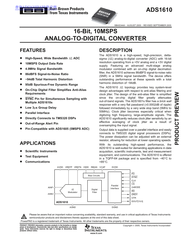
This advanced 16-bit Analog-to-Digital Converter is designed for high-speed data acquisition applications requiring exceptional precision. Operating up to 10MSPS, it features low clock jitter sensitivity and a parallel interface that easily connects with DSPs like the TMS320 series. Ideal for scientific instruments, test equipment, and communications systems. This technical documentation provides comprehensive details on electrical characteristics, operational parameters, physical constraints, and application guidelines necessary for integrating this high-performance ADC into demanding systems.
📄 Preview PAGE OF 23

Page 1 Text Content

查询ADS1610IPAPR供应商

ADS1610

SBAS344A − AUGUST 2005 − REVISED SEPTEMBER 2005

16-Bit, 10MSPS

ANALOG-TO-DIGITAL CONVERTER

FEATURES DESCRIPTION

The ADS1610 is a high-speed, high-precision, delta-

High-Speed, Wide Bandwidth ∆Σ ADC sigma (∆Σ) analog-to-digital converter (ADC) with 16-bit

resolution operating from a +5V analog and a +3V digital

10MSPS Output Data Rate

supply. Featuring an advanced multi-stage analog

4.9MHz Signal Bandwidth modulator combined with an on-chip digital decimation

filter, the ADS1610 achieves 86d BFS signal-to-noise ratio

86d BFS Signal-to-Noise Ratio

(SNR) in a 5MHz signal bandwidth. The device offers

−94d B Total Harmonic Distortion outstanding performance at these speeds with a total

harmonic distortion of −94d B.

95d B Spurious-Free Dynamic Range

The ADS1610 ∆Σ topology provides key system-level

On-Chip Digital Filter Simplifies Anti-Alias

design advantages with respect to anti-alias filtering and

Requirements

clock jitter. The design of the anti-alias filter is simplified since the on-chip digital filter greatly attenuates

SYNC Pin for Simultaneous Sampling with

out-of-band signals. The ADS1601s filter has a brick wall

Multiple ADS1610s

response with a very flat passband (±0.0002d B of ripple)

Low 3µs Group Delay followed immediately by a very wide stop band (5MHz to

55MHz). Clock jitter becomes especially critical when

Parallel Interface

digitizing high frequency, large-amplitude signals. The

Directly Connects to TMS320 DSPs ADS1610 significantly reduces clock jitter sensitivity by an

effective averaging of clock jitter as a result of

Out-of-Range Alert Pin

oversampling the input signal.

Pin-Compatible with ADS1605 (5MSPS ADC)

Output data is supplied over a parallel interface and easily connects to TMS320 digital signal processors (DSPs). The power dissipation can be adjusted with an external resistor, allowing for reduction at lower operating speeds.

APPLICATIONS

With its outstanding high-speed performance, the ADS1610 is well-suited for demanding applications in data

Scientific Instruments acquisition, scientific instruments, test and measurement

equipment, and communications. The ADS1610 is offered

Test Equipment

in a TQFP-64 package and is specified from −40°C to

Communications +85°C.

VREFP VREFN VMID RBIAS VCAPAVDD DVDD

Bias Circuits

SYNC IE CLK CS

Parallel

AINP 2x MODE

Interface

∆Σ Digital

Modulator Filter

AINN DRDY

OTR DOUT[15:0]ADS1610

AGND DGND

Please be aware that an important notice concerning availability, standard warranty, and use in critical applications of Texas Instruments semiconductor products and disclaimers thereto appears at the end of this data sheet. Power PAD is a registered trademark of Texas Instruments. All other trademarks are the property of their respective owners.

Copyright  2005, Texas Instruments Incorporated

www.ti.com

Page Summary Contents For Texas Instruments ADS1610 User's Manual and Technical Specifications

Page 1 查询ADS1610IPAPR供应商 ADS1610 SBAS344A − AUGUST 2005 − REVISED SEPTEMBER 2005 16-Bit, 10MSPS ANALOG-TO-DIGITAL CONVERTER FEATURES DESCRIPTION The ADS1610 is a high-speed, high-precision, delta- High-Speed...
Page 2 "#$%$& IE www.ti.com SBAS344A − AUGUST 2005 − REVISED SEPTEMBER 2005 This integrated circuit can be damaged by ESD. Texas ABSOLUTE MAXIMUM RATINGS Instruments recommends that all integrated ...
Page 3 www.ti.com SBAS344A − AUGUST 2005 − REVISED SEPTEMBER 2005 ELECTRICAL CHARACTERISTICS All specifications at −40°C to +85°C, AVDD = 5V, DVDD = 3V, f CLK = 60MHz, VREF = +3V, 2x MODE = low, VCM = 2.5V, ...
Page 4 "#$%$& IE www.ti.com SBAS344A − AUGUST 2005 − REVISED SEPTEMBER 2005 ELECTRICAL CHARACTERISTICS (continued) All specifications at −40°C to +85°C, AVDD = 5V, DVDD = 3V, f CLK = 60MHz, VREF = ...
Page 5 www.ti.com SBAS344A − AUGUST 2005 − REVISED SEPTEMBER 2005 PIN CONFIGURATION Top View HTQFP AGND NC AVDD NC AGND NC AINN NC AINP DOUT[15] AGND DOUT[14] AVDD DOUT[13] RBIAS DOUT[12] ADS1610 AGND DOUT[1...
Page 6 "#$%$& IE www.ti.com SBAS344A − AUGUST 2005 − REVISED SEPTEMBER 2005 PIN FUNCTION DESCRIPTION ANALOG/DIGITAL PIN NAME PIN # INPUT/OUTPUT DESCRIPTION AGND 1, 3, 6, 9, 11, 55 Analog Analog Gro...
Page 7 www.ti.com SBAS344A − AUGUST 2005 − REVISED SEPTEMBER 2005 TIMING SPECIFICATIONS DRDY t4 t4 DOUT[15:0] Data Data Data Figure 1. Data Retrieval Timing RD, CS DOUT[15:0] Figure 2. DOUT Inactive/Active T...
Page 8 "#$%$& IE www.ti.com SBAS344A − AUGUST 2005 − REVISED SEPTEMBER 2005 Timing Specifications SYMBOL DESCRIPTION MIN TYP MAX UNITS t1 CLK Period (1/f CLK) TBD 16.667 ns 1/t1 f CLK TBD MHz t2 CL...
Page 9 www.ti.com SBAS344A − AUGUST 2005 − REVISED SEPTEMBER 2005 TYPICAL CHARACTERISTICS lit ud (d lit ud (d lit ud (d At TA = +25°C, RBIAS = 18kΩ, AVDD = 5V, DVDD = 3V, f CLK = 60MHz, VREF = 3V, and VCM = ...
Page 10 "#$%$& IE www.ti.com SBAS344A − AUGUST 2005 − REVISED SEPTEMBER 2005 TYPICAL CHARACTERISTICS (continued) At TA = +25°C, RBIAS = 18kΩ, AVDD = 5V, DVDD = 3V, f CLK = 60MHz, VREF = 3V, and VCM ...
Page 11 www.ti.com SBAS344A − AUGUST 2005 − REVISED SEPTEMBER 2005 The ADS1610 supports a very wide range of input signals. OVERVIEW Having such a wide input range makes out-of-range signals unlikely. However...
Page 12 "#$%$& IE www.ti.com SBAS344A − AUGUST 2005 − REVISED SEPTEMBER 2005 INPUT CIRCUITRY Figure 7 and Figure 8 show the recommended circuits when using single-ended or differential op amps, The ...
Page 13 www.ti.com SBAS344A − AUGUST 2005 − REVISED SEPTEMBER 2005 VIN AINP VCM 100p F ADS1610THS4503 Figure 8. Recommended Single-Ended to Differential Conversion Circuit Using the THS4503 Differential Ampli...
Page 14 "#$%$& IE www.ti.com SBAS344A − AUGUST 2005 − REVISED SEPTEMBER 2005 CLOCK INPUT (CLK) Table 2. Output Code Versus Input Signal The ADS1610 uses an external clock signal to be applied INPUT ...
Page 15 www.ti.com SBAS344A − AUGUST 2005 − REVISED SEPTEMBER 2005 OUT-OF-RANGE INDICATION (OTR) DRDY outputs updating simultaneously. After synchronization, allow 55 DRDY cycles (t12) for output If the outpu...
Page 16 "#$%$& IE www.ti.com et tli ng rr SBAS344A − AUGUST 2005 − REVISED SEPTEMBER 2005 SETTLING TIME The settling time is an important consideration when measuring signals with large steps or whe...
Page 17 www.ti.com SBAS344A − AUGUST 2005 − REVISED SEPTEMBER 2005 ag ni tu de (d ag ni tu de (d Figure 15 shows the passband ripple from DC to 4.4MHz (f CLK = 60MHz). Figure 16 shows a closer view of the pas...
Page 18 "#$%$& IE www.ti.com SBAS344A − AUGUST 2005 − REVISED SEPTEMBER 2005 POWER-DOWN (PD) POWER SUPPLIES When not in use, the ADS1610 can be powered down by Two supplies are used on the ADS1610: ...
Page 19 www.ti.com SBAS344A − AUGUST 2005 − REVISED SEPTEMBER 2005 2X MODE Two approaches can be used for the ground planes: either a single common plane; or two separate planes, one for the The 2x MODE digit...
Page 20 "#$%$& IE www.ti.com SBAS344A − AUGUST 2005 − REVISED SEPTEMBER 2005 APPLICATIONS INFORMATION INTERFACING THE ADS1610 TO THE TMS320C5400 INTERFACING THE ADS1610 TO THE Figure 21 illustrates ...
Page 21 PACKAGE OPTION ADDENDUM www.ti.com 2-Sep-2005 PACKAGING INFORMATION Orderable Device Status Package Package Pins Package Eco Plan Lead/Ball Finish MSL Peak Temp Type Drawing Qty ADS1610IPAPR PREVIEW H...
Page 23 IMPORTANT NOTICE Texas Instruments Incorporated and its subsidiaries (TI) reserve the right to make corrections, modifications, enhancements, improvements, and other changes to its products and servic...

Manual Details

Brand Texas Instruments
Pages 23
File Size 305.99 KB
Published June 16, 2026
7 views

Enter the captcha to get the download link:

captcha

Frequently Asked Questions

What is the maximum output data rate?

10MSPS Output Data Rate.

What applications is the ADS1610 suited for?

Scientific Instruments, Test Equipment, Communications.

What is the operating temperature range?

Operates from -40°C to +85°C.

What signal-to-noise ratio does it achieve?

86dBFS Signal-to-Noise Ratio.