# A B C D E F G H I J K L M N O P Q R S T U V W X Y Z

ST VNQ830PEP-ES High Side Driver for Quad Channel Applications - Data Sheet/User Guide

Summary

This manual provides comprehensive details for the VNQ830PEP-E, a quad-channel high side driver designed for robust power management systems. Key features include advanced protection against open/shorted loads, overvoltage/undervoltage spikes, ground loss, and reverse battery flow. The guide covers electrical specifications, thermal data, application circuits (like load dump and GND protection), making it essential reading for electrical engineers designing reliable automotive or industrial DC-DC conversion systems requiring high levels of fault tolerance.
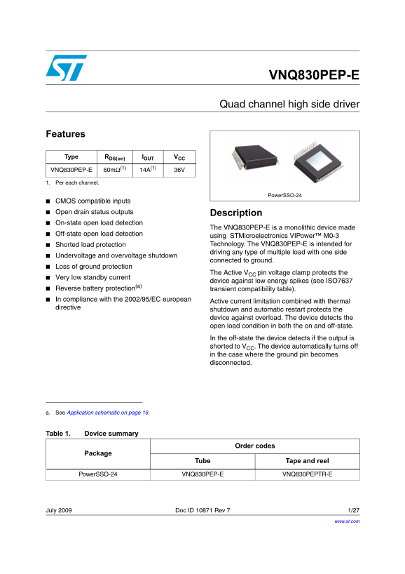
📄 Preview 📖 Table of Contents Contents PAGE OF 27

Page 1 Text Content

VNQ830PEP-E

Quad channel high side driver

Features

Type RDS(on) IOUT VCC

VNQ830PEP-E 60mΩ(1) 14A(1) 36V

1. Per each channel.

Power SSO-24

CMOS compatible inputs Open drain status outputs Description On-state open load detection

The VNQ830PEP-E is a monolithic device made

Off-state open load detection

using| STMicroelectronics VIPower™ M0-3 Shorted load protection Technology. The VNQ830PEP-E is intended for driving any type of multiple load with one side

Undervoltage and overvoltage shutdown

connected to ground.

Loss of ground protection

The Active VCC pin voltage clamp protects the

Very low standby current

device against low energy spikes (see ISO7637

Reverse battery protection(a) transient compatibility table). In compliance with the 2002/95/EC european

Active current limitation combined with thermal

directive

shutdown and automatic restart protects the device against overload. The device detects the open load condition in both the on and off-state. In the off-state the device detects if the output is shorted to VCC. The device automatically turns off in the case where the ground pin becomes disconnected.

a. See Application schematic on page

Table 1. Device summary

Order codes

Package

Tube Tape and reel

Power SSO-24 VNQ830PEP-E VNQ830PEPTR-E

July 2009 Doc ID 10871 Rev 7 1/27

www.st.com

Page Summary Contents For ST VNQ830PEP-ES High Side Driver for Quad Channel Applications - Data Sheet/User Guide

Page 1 VNQ830PEP-E Quad channel high side driver Features Type RDS(on) IOUT VCC VNQ830PEP-E 60mΩ(1) 14A(1) 36V 1. Per each channel. Power SSO-24 CMOS compatible inputs Open drain status outputs Description O...
Page 2 Contents VNQ830PEP-E Contents Block diagram and pin description . . . . . . . . . . . . . . . . . . . . . . . . . . . . . 5 Electrical specifications . . . . . . . . . . . . . . . . . . . . . . . . . ...
Page 3 VNQ830PEP-E List of tables List of tables Table 1. Device summary . . . . . . . . . . . . . . . . . . . . . . . . . . . . . . . . . . . . . . . . . . . . . . . . . . . . . . . . . . 1 Table 2. Suggest...
Page 4 List of figures VNQ830PEP-E List of figures Figure 1. Block diagram . . . . . . . . . . . . . . . . . . . . . . . . . . . . . . . . . . . . . . . . . . . . . . . . . . . . . . . . . . . . 5 Figure 2. ...
Page 5 VNQ830PEP-E Block diagram and pin description 1 Block diagram and pin description Figure 1. Block diagram VCC OUTPUT1OVERVOLTAGE CLAMP VCC UNDERVOLTAGE INPUT2 CONTROL & PROTECTION STATUS2 EQUIVALE...
Page 6 Electrical specifications VNQ830PEP-E 2 Electrical specifications 2.1 Absolute maximum ratings Stressing the device above the rating listed in the “Absolute maximum ratings” table may cause permanent ...
Page 7 VNQ830PEP-E Electrical specifications 2.3 Electrical characteristics Values specified in this section are for 8V < VCC < 36V; -40°C < Tj < 150°C, unless otherwise stated. Figure 3. Current...
Page 8 Electrical specifications VNQ830PEP-E Table 5. Power output (continued) Symbol Parameter Test conditions Min. Typ. Max. Unit VIN = VOUT = 0V; VCC = 13V; IL(off3) Off-state output current µA Tj = 125°C...
Page 9 VNQ830PEP-E Electrical specifications Table 9. Logic inputs Symbol Parameter Test conditions Min. Typ. Max. Unit VIL Input low level 1.25 IIL Low level input current VIN = 1.25V µA VIH Input high leve...
Page 10 Electrical specifications VNQ830PEP-E Figure 5. Switching characteristics VOUTn d VOUT/dt(off) d VOUT/dt(on) td(on) td(off) Table 12. Truth table Conditions Input Output Status Normal operation Curren...
Page 11 VNQ830PEP-E Electrical specifications Table 13. Electrical transient requirements (part 1/3) ISO T/R Test level II III IV Delays and impedance Test pulse - 25V - 50V - 75V - 100V 2ms, 10Ω + 25V + 50V ...
Page 12 Electrical specifications VNQ830PEP-E Figure 6. Waveforms NORMAL OPERATION INPUTn OUTPUT VOLTAGEn STATUSn UNDERVOLTAGE VCC VUSDhyst INPUTn OUTPUT VOLTAGEn STATUSn undefined OVERVOLTAGE VCC<VOV VCC&...
Page 13 VNQ830PEP-E Electrical specifications 2.4 Electrical characteristics curves Figure 7. Off-state output current Figure 8. High level input current IL (off1) (µA) Iih (µA) 2.8 Vcc=13V Vcc=36 2.1 Vin=3.2...
Page 14 Electrical specifications VNQ830PEP-E Figure 13. ILIM vs Tcase Figure 14. On-state resistance vs VCC Ilim (A) Ron (m Ohm) Iout=2A Vcc=13V Tc=150°C Tc=25°C Tc=-40°C Tc (°C) Vcc (V) Figure 15. Input hig...
Page 15 VNQ830PEP-E Electrical specifications Figure 19. Status leakage current Figure 20. Status low output voltage Istat (n A) Vstat (V) 0.8 Vstat=5V Istat=1.6m A Tc (°C) Tc (°C) Figure 21. Status clamp vol...
Page 16 Application information VNQ830PEP-E 3 Application information Figure 24. Application schematic Rprot STATUSn μC Rprot INPUTn OUTPUTn VGND DGND 3.1 GND protection network against reverse battery This s...
Page 17 VNQ830PEP-E Application information Please note that, if the microprocessor ground is not shared by the device ground, then the RGND will produce a shift (IS(on)max * RGND) in the input thresholds and...
Page 18 Application information VNQ830PEP-E 3.4 Open-load detection in off-state Off-state open load detection requires an external pull-up resistor (RPU) connected between OUTPUT pin and a positive supply vo...
Page 19 VNQ830PEP-E Application information 3.5 Maximum demagnetization energy (VCC = 13.5V) Figure 26. Maximum turn-off current versus load inductance ILMAX (A) A = single pulse at TJstart = 150ºC B= repetit...
Page 20 Package and PC board thermal data VNQ830PEP-E 4 Package and PC board thermal data 4.1 Power SSO-24 thermal data Figure 27. Power SSO-24 PC board Note: Layout condition of Rth and Zth measurements (PCB...
Page 21 VNQ830PEP-E Package and PC board thermal data Figure 29. Power SSO-24 thermal impedance junction ambient single pulse (one channel ON) ZTH (°C/W) Footprint 8 cm2 Time (s) Figure 30. Thermal fitting mo...
Page 22 Package and PC board thermal data VNQ830PEP-E Equation 1: pulse calculation formula: ZTHδ RTH ZTHtp δ–( )+⋅= where δ = t P/T Table 16. Thermal parameters Area/island (cm2) Footprint 22/27 Doc ID 10871...
Page 23 VNQ830PEP-E Package and packing information 5 Package and packing information 5.1 ECOPACK® packages In order to meet environmental requirements, ST offers these devices in different grades of ECOPACK®...
Page 24 Package and packing information VNQ830PEP-E Table 17. Power SSO-24 mechanical data(1) (2) Millimeters Symbol Min. Typ. Max. 1. No intrusion allowed inwards the leads. 2. Flash or bleeds on exposed die...
Page 25 VNQ830PEP-E Package and packing information 5.3 Packing information Figure 32. Power SSO-24 tube shipment (no suffix) Base Q.ty Bulk Q.ty Tube length (± 0.5) C (± 0.1) 0.6 All dimensions are in mm. Fi...
Page 26 Revision history VNQ830PEP-E 6 Revision history Table 18. Document revision history Date Revision Changes 10-Nov-2004 Initial release. 22-Nov-2006 Pdf changed. Mechanical data updating. 07-Dec-2004 Po...
Page 27 VNQ830PEP-E Please Read Carefully: Information in this document is provided solely in connection with ST products. STMicroelectronics NV and its subsidiaries (“ST”) reserve the right to make changes, ...

Manual Details

Brand QUAD
Pages 27
File Size 405.87 KB
Published June 04, 2026
59 views

Enter the captcha to get the download link:

captcha

Frequently Asked Questions

How does the VNQ830PEP-E detect an open load in the off-state?

The device detects if the output is shorted to V, while also providing automatic shutdown if ground becomes disconnected.

What protective measures are built into the driver against overload and spikes?

It features active current limitation combined with thermal shutdown/restart, plus low standby current and root cause protection.

What methods should be used for GND protection against a reverse battery?

You must either place a resistor on the ground line (RGND only) or use a diode (D) in the ground line.

Is this high side driver compatible with microcontrollers (MCUs)?

Yes, it includes CMOS compatible inputs and provides MCU I/O protection.