# A B C D E F G H I J K L M N O P Q R S T U V W X Y Z

ST VND5E025BK-E Dual Channel High-Side Driver with Analog Current Sensing for Automotive Applications

Summary

The VND5E025BK-E is a robust double channel high-side driver designed specifically for demanding automotive applications. Featuring integrated analog current sensing, it offers advanced protection against diverse faults including overvoltage clamp, thermal shutdown, and overload. This manual provides comprehensive system documentation, detailing electrical specifications, specialized application guidance (including setup for various protective networks like GND and load dump), ensuring easy and reliable integration of the device into high-precision automotive and embedded systems.
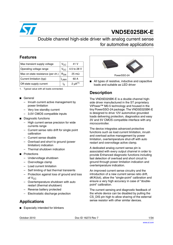
📄 Preview 📖 Table of Contents Contents PAGE OF 34

Page 1 Text Content

VND5E025BK-E

Double channel high-side driver with analog current sense

for automotive applications

Features Max transient supply voltage VCC

Operating voltage range VCC 4.5 to 28

Max on-state resistance (per ch.) RON mΩ

Power SSO-24

Current limitation (typ) ILIMH

All types of resistive, inductive and capacitive

Off-state supply current IS µA(1)

loads and suitable as LED driver

1. Typical value with all loads connected.

Description

General

The VND5E025BK-E is a double channel high-

Inrush current active management by side driver manufactured in the ST proprietary power limitation VIPower™ M0-5 technology and housed in the

Very low standby current tiny Power SSO-24 package. The VND5E025BK-E is designed to drive 12V automotive grounded

3.0V CMOS compatible inputs

loads delivering protection, diagnostics and easy

Diagnostic functions

3V and 5V CMOS compatible interface with any

High current sense precision for wide

microcontroller.

currents range

The device integrates advanced protective

Current sense ratio drift for single point

functions such as load current limitation, inrush

calibration

and overload active management by power

Current sense disable

limitation, overtemperature shut-off with auto

Overload and short to ground (power

restart and overvoltage active clamp.

limitation) indication

A dedicated analog current sense pin is

Thermal shutdown indication

associated with every output channel in order to

Protections

provide Enhanced diagnostic functions including

Undervoltage shutdown fast detection of overload and short circuit to

Overvoltage clamp ground through power limitation indication and overtemperature indication.

Load current limitation Self limiting of fast thermal transients An improved current sense circuitry and the

Protection against loss of ground and loss introduction of a new current sense ratio drift, of VCC d K/K(tot), allow the "single-point" calibration and ensure a very high accuracy in case of "double-

Overtemperature shutdown with auto

point" calibration.

restart (thermal shutdown) Reverse battery protected The current sensing and diagnostic feedback of

Electrostatic discharge protection the whole device can be disabled by pulling the CS_DIS pin high to allow sharing of the external sense resistor with other similar devices.

Applications Especially intended for blinkers

October 2010 Doc ID 16273 Rev 7 1/34

www.st.com

Page Summary Contents For ST VND5E025BK-E Dual Channel High-Side Driver with Analog Current Sensing for Automotive Applications

Page 1 VND5E025BK-E Double channel high-side driver with analog current sense for automotive applications Features Max transient supply voltage VCC Operating voltage range VCC 4.5 to 28 Max on-state resistan...
Page 2 Contents VND5E025BK-E Contents Block diagram and pin description . . . . . . . . . . . . . . . . . . . . . . . . . . . . . 5 Electrical specification . . . . . . . . . . . . . . . . . . . . . . . . . ...
Page 3 VND5E025BK-E List of tables List of tables Table 1. Pin functions . . . . . . . . . . . . . . . . . . . . . . . . . . . . . . . . . . . . . . . . . . . . . . . . . . . . . . . . . . . . . 5 Table 2. S...
Page 4 List of figures VND5E025BK-E List of figures Figure 1. Block diagram . . . . . . . . . . . . . . . . . . . . . . . . . . . . . . . . . . . . . . . . . . . . . . . . . . . . . . . . . . . . 5 Figure 2....
Page 5 VND5E025BK-E Block diagram and pin description 1 Block diagram and pin description Figure 1. Block diagram Signal Clamp Undervoltage Control & Diagnostic 1 Power Clamp IN1 DRIVER IN2 VON CH 1 Limi...
Page 6 Block diagram and pin description VND5E025BK-E Figure 2. Configuration diagram (top view) OUTPUT2 GND OUTPUT2 N.C. OUTPUT2 INPUT2 OUTPUT2 N.C. OUTPUT2 INPUT1 OUTPUT2 N.C. OUTPUT1 CURRENT SENSE1 OUTPUT...
Page 7 VND5E025BK-E Electrical specification 2 Electrical specification Figure 3. Current and voltage conventions VFn VCC IOUT1 OUTPUT1 CS_DIS VCSD ISENSE1 VOUT1 CURRENT INPUT1 SENSE1 IOUT2 VSENSE1 OUTPUT2 I...
Page 8 Electrical specification VND5E025BK-E Table 3. Absolute maximum ratings (continued) Symbol Parameter Value Unit Maximum switching energy (single pulse) EMAX (L 0.8 m H; RL Ω; Vbat 13.5 V; Tjstart °C; ...
Page 9 VND5E025BK-E Electrical specification 2.3 Electrical characteristics Values specified in this section are for 8V<VCC<28V; -40°C<Tj<150°C, unless otherwise stated. Table 5. Power section Sy...
Page 10 Electrical specification VND5E025BK-E Table 7. Logic inputs Symbol Parameter Test conditions Min. Typ. Max. Unit VIL Input low level voltage 0.9 IIL Low level input current VIN 0.9V µA VIH Input high ...
Page 11 VND5E025BK-E Electrical specification Table 9. Current sense (8V VCC 18V) Symbol Parameter Test conditions Min. Typ. Max. Unit IOUT 0.05A; VSENSE 0.5V; VCSD 0V; KLED IOUT/ISENSE Tj -40°C to 150°C IOUT...
Page 12 Electrical specification VND5E025BK-E Table 9. Current sense (8V VCC 18V) (continued) Symbol Parameter Test conditions Min. Typ. Max. Unit IOUT 0A; VSENSE 0V; VCSD 5V; VIN 0V; Tj -40°C to 150°C µA Ana...
Page 13 VND5E025BK-E Electrical specification Figure 4. Current sense delay characteristics INPUT CS_DIS LOAD CURRENT SENSE CURRENT t DSENSE2H t DSENSE1H t DSENSE2Lt DSENSE1L Figure 5. Switching characteristi...
Page 14 Electrical specification VND5E025BK-E Figure 7. Delay response time between rising edge of output current and rising edge of current sense (CS enabled) Δt DSENSE2H IOUTMAX 90% IOUTMAX ISENSE ISENSEMAX...
Page 15 VND5E025BK-E Electrical specification Figure 9. Maximum current sense ratio drift vs load current d K/K(min) d K/K(max) Iout (A) Note: Parameter guaranteed by design; it is not tested. Table 10. Truth...
Page 16 Electrical specification VND5E025BK-E Table 11. Electrical transient requirements (part 1/3) Burst cycle / pulse ISO 7637-2: Test levels (1) Number of repetition time Delays and 2004(E) Test pulses or...
Page 17 VND5E025BK-E Electrical specification 2.4 Waveforms Figure 10. Normal operation Normal operation INPUT Nominal load Nominal load VSENSE VCS_DIS Figure 11. Overload or short to GND Overload or Short to...
Page 18 Electrical specification VND5E025BK-E Figure 12. Intermittent overload Intermittent Overload INPUT Overload ILim H Nominal load ILim L VSENSEH> VSENSE VCS_DIS Figure 13. TJ evolution in overload or...
Page 19 VND5E025BK-E Electrical specification 2.5 Electrical characteristics curves Figure 14. Off-state output current Figure 15. High level input current Iloff (n A) Iih (µA) Vin = 2.1V Off State VCC = 8 V ...
Page 20 Electrical specification VND5E025BK-E Figure 20. On-state resistance vs Tcase Figure 21. On-state resistance vs VCC Ron (m Ohm) Ron (m Ohm) Iout= 3A Vcc=13V Tc=150°C Tc=125°C Tc=25°C Tc=-40°C Tc (°C) ...
Page 21 VND5E025BK-E Electrical specification Figure 26. CS_DIS high level voltage Figure 27. CS_DIS low level voltage Vcsdl (V) Vcsdh (V) Tc (°C) Tc (°C) Figure 28. CS_DIS clamp voltage Vcsdcl(V) Icsd = 1 m ...
Page 22 Application information VND5E025BK-E 3 Application information Figure 29. Application schematic Rprot CS_DIS ΜCU INPUTRprot OUTPUT Rprot CURRENT SENSE RSENSE CEXT VGND DGND Note: Channel 2 has the sam...
Page 23 VND5E025BK-E Application information values. This shift will vary depending on how many devices are On in the case of several high-side drivers sharing the same RGND. If the calculated power dissipati...
Page 24 Application information VND5E025BK-E 3.4 Current sense and diagnostic The current sense pin performs a double function (see Figure 30: Current sense and diagnostic): Current mirror of the load current...
Page 25 VND5E025BK-E Application information 3.5 Maximum demagnetization energy (VCC 13.5V) Figure 31. Maximum turn-off current versus inductance (for each channel) A: Tjstart 150°C single pulse B: Tjstart 10...
Page 26 Package and thermal data VND5E025BK-E 4 Package and thermal data 4.1 Power SSO-24 thermal data Figure 32. Power SSO-24 PC board Note: Layout condition of Rth and Zth measurements (PCB: Double layer, T...
Page 27 VND5E025BK-E Package and thermal data Figure 34. Power SSO-24 thermal impedance junction to ambient single pulse (one channel on) ZTH (°C/W) Footprint 2 cm2 8 cm2 Time (s) Equation 1: pulse calculatio...
Page 28 Package and thermal data VND5E025BK-E Table 14. Thermal parameters Area/Island (cm2) Footprint 28/34 Doc ID 16273 Rev 7
Page 29 VND5E025BK-E Package and packing information 5 Package and packing information 5.1 ECOPACK® In order to meet environmental requirements, ST offers these devices in different grades of ECOPACK® package...
Page 30 Package and packing information VND5E025BK-E Table 15. Power SSO-24 mechanical data Millimeters Symbol Min. Typ. Max. 5.3 Packing information Figure 37. Power SSO-24 tube shipment (no suffix) Base Qty...
Page 31 VND5E025BK-E Package and packing information Figure 38. Power SSO-24 tape and reel shipment (suffix “TR”) REEL DIMENSIONS Base Qty Bulk Qty A (max) B (min) 1.5 C (±0.2) G (+2 / -0) 24.4 N (min) T (max...
Page 32 Order codes VND5E025BK-E 6 Order codes Table 16. Device summary Order codes Package Tube Tape and reel Power SSO-24 VND5E025BK-E VND5E025BKTR-E 32/34 Doc ID 16273 Rev 7
Page 33 VND5E025BK-E Revision history 7 Revision history Table 17. Document revision history Date Revision Changes 17-Sep-2009 Initial release. 02-Nov-2009 Updated Table 5: Power section. Updated Table 9: Cur...
Page 34 VND5E025BK-E Please Read Carefully: Information in this document is provided solely in connection with ST products. STMicroelectronics NV and its subsidiaries (“ST”) reserve the right to make changes,...

Manual Details

Brand Current
Pages 34
File Size 572.77 KB
Published June 03, 2026
71 views

Enter the captcha to get the download link:

captcha

Frequently Asked Questions

What is the maximum transient supply voltage (VCC)?

The maximum transient supply voltage is 41 V.

How can I protect against reverse battery current?

You must either place a resistor in the ground line (RGND) or use a diode (DGND).

What types of protective functions are integrated into this driver?

It provides overload, undervoltage shutdown, overtemperature detection, and reverse battery protection.

Can this device drive various electrical loads?

Yes, it is suitable for resistive, inductive, capacitive loads, and works as an LED driver.