# A B C D E F G H I J K L M N O P Q R S T U V W X Y Z

ST VNQ830P-E Quad channel high-side driver Data Sheet User Manual

Summary

The VNQ830P-E is a highly reliable quad high-side driver designed for robust power management applications requiring multiple load output control. Featuring comprehensive built-in protection, including thermal shutdown, over/undervoltage clamping, and open-load detection in both on and off states, this unit meets rigorous automotive grade standards. This manual provides detailed electrical specifications, application guidelines (such as ground and load dump protection), and system integration advice for engineers building durable electronic systems.
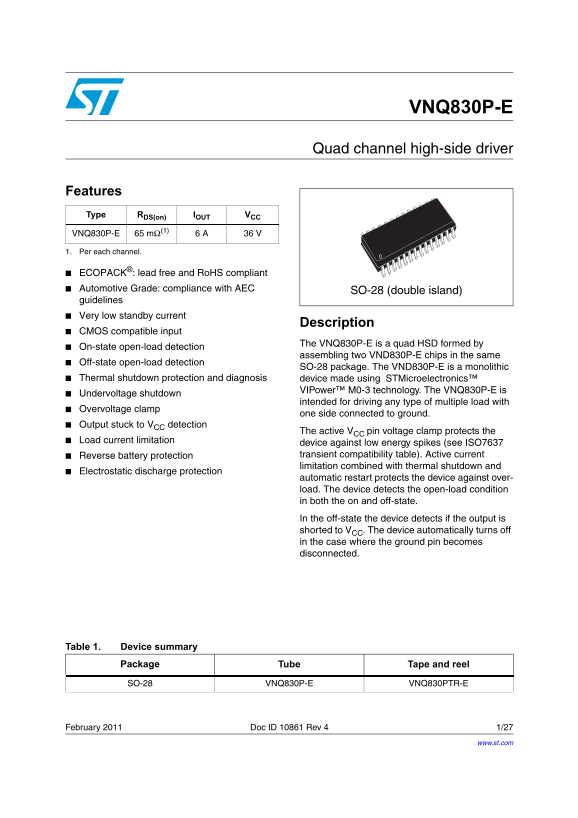
📄 Preview 📖 Table of Contents Contents PAGE OF 27

Page 1 Text Content

VNQ830P-E

Quad channel high-side driver

Features Type RDS(on) IOUT VCC VNQ830P-E mΩ(1) 1. Per each channel.

ECOPACK®: lead free and Ro HS compliant Automotive Grade: compliance with AEC SO-28 (double island) guidelines Very low standby current

Description

CMOS compatible input

The VNQ830P-E is a quad HSD formed by

On-state open-load detection

assembling two VND830P-E chips in the same

Off-state open-load detection

SO-28 package. The VND830P-E is a monolithic

Thermal shutdown protection and diagnosis device made using| STMicroelectronics™

VIPower™ M0-3 technology. The VNQ830P-E is

Undervoltage shutdown

intended for driving any type of multiple load with

Overvoltage clamp

one side connected to ground.

Output stuck to VCC detection

The active VCC pin voltage clamp protects the

Load current limitation

device against low energy spikes (see ISO7637 Reverse battery protection transient compatibility table). Active current limitation combined with thermal shutdown and

Electrostatic discharge protection

automatic restart protects the device against over- load. The device detects the open-load condition in both the on and off-state. In the off-state the device detects if the output is shorted to VCC. The device automatically turns off in the case where the ground pin becomes disconnected.

Table 1. Device summary

Package Tube Tape and reel

SO-28 VNQ830P-E VNQ830PTR-E

February 2011 Doc ID 10861 Rev 4 1/27

www.st.com

Page Summary Contents For ST VNQ830P-E Quad channel high-side driver Data Sheet User Manual

Page 1 VNQ830P-E Quad channel high-side driver Features Type RDS(on) IOUT VCC VNQ830P-E mΩ(1) 1. Per each channel. ECOPACK®: lead free and Ro HS compliant Automotive Grade: compliance with AEC SO-28 (double ...
Page 2 VNQ830P-E Contents Contents Block diagram and pin description . . . . . . . . . . . . . . . . . . . . . . . . . . . . . 5 Electrical specifications . . . . . . . . . . . . . . . . . . . . . . . . . . ...
Page 3 VNQ830P-E List of tables List of tables Table 1. Device summary . . . . . . . . . . . . . . . . . . . . . . . . . . . . . . . . . . . . . . . . . . . . . . . . . . . . . . . . . . 1 Table 2. Suggested...
Page 4 VNQ830P-E List of figures List of figures Figure 1. Block diagram . . . . . . . . . . . . . . . . . . . . . . . . . . . . . . . . . . . . . . . . . . . . . . . . . . . . . . . . . . . . 5 Figure 2. Co...
Page 5 VNQ830P-E Block diagram and pin description 1 Block diagram and pin description Figure 1. Block diagram VCC1,2 OVERVOLTAGE CLAMP UNDERVOLTAGE GND1,2 CLAMP 1 OUTPUT1 INPUT1 DRIVER 1 CLAMP 2 STATUS1 CUR...
Page 6 VNQ830P-E Block diagram and pin description Figure 2. Configuration diagram (top view) VCC1,2 VCC1,2 GND 1,2 OUTPUT1 INPUT1 OUTPUT1 STATUS1 OUTPUT1 STATUS2 OUTPUT2 INPUT2 OUTPUT2 VCC1,2 OUTPUT2 VCC3,4...
Page 7 VNQ830P-E Electrical specifications 2 Electrical specifications 2.1 Absolute maximum ratings Stressing the device above the rating listed in Table 3 may cause permanent damage to the device. These are...
Page 8 VNQ830P-E Electrical specifications 2.2 Thermal data Table 4. Thermal data (per island) Symbol Parameter Value Unit Rthj-lead Thermal resistance junction-lead 15 °C/W Thermal resistance junction-ambie...
Page 9 VNQ830P-E Electrical specifications Table 5. Power (continued) Symbol Parameter Test conditions Min. Typ. Max. Unit IOUT = 2 A; Tj = 25°C mΩ RON On-state resistance IOUT = 2 A; VCC > 8 mΩ Off-state...
Page 10 VNQ830P-E Electrical specifications Table 8. Switching (VCC = 13V; Tj = 25°C) Symbol Parameter Test conditions Min. Typ. Max. Unit RL = 6.5Ω from VIN rising td(on) Turn-on delay time edge to VOUT = 1....
Page 11 VNQ830P-E Electrical specifications Table 11. Open-load detection Symbol Parameter Test conditions Min. Typ. Max. Unit Open-load on-state detection IOL VIN = 5 V 50 m A threshold Open-load on-state de...
Page 12 VNQ830P-E Electrical specifications Table 12. Truth table Conditions Input Output Status Normal operation Current limitation (Tj < TTSD) H (Tj > TTSD) L Overtemperature Undervoltage Overvoltage ...
Page 13 VNQ830P-E Electrical specifications Figure 6. Waveforms NORMAL OPERATION INPUTn LOAD VOLTAGEn STATUSn UNDERVOLTAGE VCC VUSDhyst INPUTn LOAD VOLTAGEn STATUS undefined OVERVOLTAGE VCC<VOV VCC > VO...
Page 14 VNQ830P-E Electrical specifications 2.4 Electrical characteristics curves Figure 7. Off-state output current Figure 8. High level input current IL(off1) (u A) Iih (u A) Off state Vin=3.25V Vcc=36V Vin...
Page 15 VNQ830P-E Electrical specifications Figure 13. ILIM vs Tcase Figure 14. On-state resistance vs VCC Ilim (A) Ron (m Ohm) Tc=150°C Vcc=13V Tc=25°C Tc= - 40°C Iout=2A Tc (°C) Vcc (V) Figure 15. Input hig...
Page 16 VNQ830P-E Electrical specifications Figure 19. Status leakage current Figure 20. Status low output voltage Ilstat (u A) Vstat (V) 0.04 Istat=1.6m A Vstat=5V Tc (°C) Tc (°C) Figure 21. Status clamp vol...
Page 17 VNQ830P-E Application information 3 Application information Figure 24. Application schematic VCC1,2 VCC3,4 Rprot STATUS1 Rprot INPUT1 Rprot STATUS2 OUTPUT1 Rprot INPUT2 OUTPUT2 Rprot STATUS3 Rprot OUT...
Page 18 VNQ830P-E Application information where - IGND is the DC reverse ground pin current and can be found in the absolute maximum rating section of the device datasheet. Power dissipation in RGND (when VCC...
Page 19 VNQ830P-E Application information Example For the following conditions: VCCpeak = - 100 Ilatchup ≥ 20 m A VOHμC ≥ 4.5 kΩ ≤ Rprot ≤ 65 kΩ. Recommended values are: Rprot = 10 kΩ 3.4 Open-load detection ...
Page 20 VNQ830P-E Application information 3.5 Maximum demagnetization energy (VCC = 13.5 V) Figure 26. Maximum turn-off current versus load inductance ILM AX (A) A = single pulse at TJstart = 150ºC B= repetit...
Page 21 VNQ830P-E Package and PCB thermal data 4 Package and PCB thermal data 4.1 SO-28 thermal data Figure 27. SO-28 PC board Note: Layout condition of Rth and Zth measurements (PCB FR4 area = 58 mm x 58 mm,...
Page 22 VNQ830P-E Package and PCB thermal data Figure 28. Rthj-amb vs PCB copper area in open box free air condition RTHj_amb (°C/W) Rth A Rth B Rth C PCB Cu heatsink area (cm^2)/island Figure 29. SO-28 therm...
Page 23 VNQ830P-E Package and PCB thermal data Equation 1: pulse calculation formula ZTHδ RTH ZTHtp δ–( )+⋅= where tp T⁄= Figure 30. Thermal fitting model of a quad channel HSD in SO-28 Tj_2 C13 C14 Tj_3 C7 C...
Page 24 VNQ830P-E Package and packing information 5 Package and packing information 5.1 ECOPACK® packages In order to meet environmental requirements, ST offers these devices in different grades of ECOPACK® p...
Page 25 VNQ830P-E Package and packing information 5.2 SO-28 packing information Figure 32. SO-28 tube shipment (no suffix) Base Q.ty Bulk Q.ty Tube length (± 0.5) All dimensions are in mm. Figure 33. SO-28 ta...
Page 26 VNQ830P-E Revision history 6 Revision history Replaced Table 17. Document revision history Date Revision Changes 03-May-2006 Initial release. Document reformatted and restructured. 18-Dec-2008 Added c...
Page 27 VNQ830P-E Please Read Carefully: Information in this document is provided solely in connection with ST products. STMicroelectronics NV and its subsidiaries (“ST”) reserve the right to make changes, co...

Manual Details

Brand QUAD
Pages 27
File Size 399.11 KB
Published June 04, 2026
36 views

Enter the captcha to get the download link:

captcha

Frequently Asked Questions

What types of protection features does the VNQ830P-E provide?

It offers overvoltage clamps, thermal shutdown, ESD protection, load dump protection, and open-load detection in both on and off states.

How should I implement reverse battery protection for the ground line (GND)?

You can use either a resistor in the ground line or a diode placed in the ground line path.

Is this device rated for vehicle applications?

Yes, it features Automotive Grade compliance guidelines and is suitable for connecting to negative Lish Energy Spikes.

Does the device detect if the output is shorted to V when the system is off?

Yes, in the off-state, the device detects if the output is shorted to V. The active V pin voltage clamp protects the CC output.