ST L6376 0.5A HIGH-SIDE DRIVER QUAD INTELLIGENT POWER SWITCH
Summary
The L6376 is a high-reliability quad Intelligent Power Switch utilizing advanced Multipower BCD technology. It provides four independent outputs designed for robust switching of general industrial loads (inductive, capacitive, or resistive). The unit features comprehensive protection mechanisms, including thermal shutdown, undervoltage lockout, and non-dissipative over-current limiting. This manual offers detailed specifications, operational diagrams, and control parameters, making it essential for electronics engineers designing durable, high-performance equipment that requires reliable power management in demanding industrial environments.
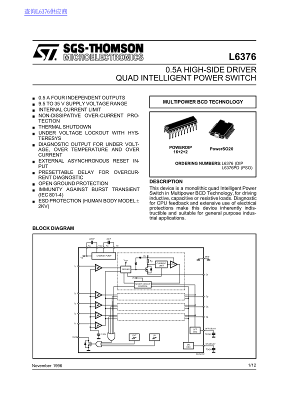
Page 1 Text Content
0.5A HIGH-SIDE DRIVER
QUAD INTELLIGENT POWER SWITCH
0.5 FOUR INDEPENDENT OUTPUTS
MULTIPOWER BCD TECHNOLOGY
9.5 TO SUPPLY VOLTAGE RANGE INTERNAL CURRENT LIMIT NON-DISSIPATIVE OVER-CURRENT PRO- TECTION THERMAL SHUTDOWN UNDER VOLTAGE LOCKOUT WITH HYS- TERESYS DIAGNOSTIC OUTPUT FOR UNDER VOLT-
POWERDIP
AGE, OVER TEMPERATURE AND OVER Power SO20
CURRENT EXTERNAL ASYNCHRONOUS RESET IN-
ORDERING NUMBERS:L6376 (DIP
L6376PD (PSO)
PRESETTABLE DELAY FOR OVERCUR- RENT DIAGNOSTIC
DESCRIPTION
OPEN GROUND PROTECTION
This device is monolithic quad Intelligent Power
IMMUNITY AGAINST BURST TRANSIENT
Switch in Multipower BCD Technology, for driving
(IEC 801-4)
inductive, capacitive or resistive loads. Diagnostic
ESD PROTECTION (HUMAN BODY MODEL
for CPU feedback and extensive use of electrical
protections make this device inherently indis- tructible and suitable for general purpose indus- trial applications.
BLOCK DIAGRAM
VCPVS VC VP
CHARGE PUMP VS GND
VCP RS
CURRENT OVC I1 LIMIT
DRIVER
SHORT CIRCUIT CONTROL
OFF OFF DELAY
1.25V CDOFF
OVT UV
ON ON DELAY
D94IN076C
November 1/12
Page Summary Contents For ST L6376 0.5A HIGH-SIDE DRIVER QUAD INTELLIGENT POWER SWITCH
Manual Details
| Brand | QUAD |
|---|---|
| Pages | 12 |
| File Size | 112.34 KB |
| Published | June 04, 2026 |
Enter the captcha to get the download link:

Frequently Asked Questions
What types of loads can the L6376 device drive?
It is designed for driving inductive, capacitive, or resistive loads according to IEC 801-4 standards.
What protection features are built into this switch?
The device includes features such as internal current limitation, over-current protection, thermal shutdown, and undervoltage lockout.
How can I monitor the status of the L6376?
The DIAG pin is an open drain output that reports the IC's working condition, turning low when issues like undervoltage, overcurrent, or overtemperature occur.