# A B C D E F G H I J K L M N O P Q R S T U V W X Y Z

ST VN5016AJ-E High Side Driver with Analog Current Sense for Automotive Applications - Data Sheet User Manual

Summary

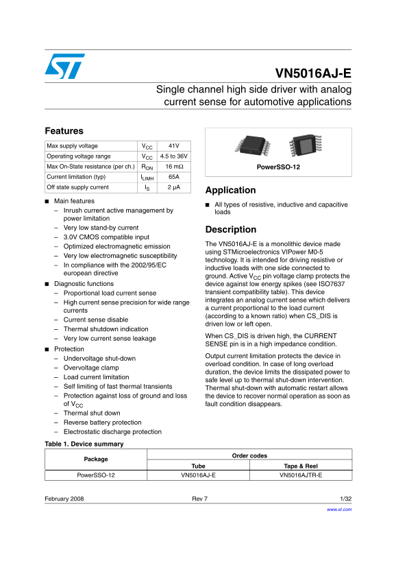
The VN5016AJ-E is a robust single-channel high side driver featuring integrated analog current sensing, designed specifically for demanding automotive applications. It manages various loads (resistive, inductive, capacitive) while providing critical protection against faults like overvoltage, thermal extremes, and reverse battery currents. This manual serves as a comprehensive technical guide, covering detailed electrical specifications, application information, and grounding solutions, making it essential for engineers designing reliable power systems requiring precise current monitoring and maximum fault tolerance.
📄 Preview 📖 Table of Contents Contents PAGE OF 32

Page 1 Text Content

VN5016AJ-E

Single channel high side driver with analog current sense for automotive applications

Features Max supply voltage VCC 41V

Operating voltage range VCC 4.5 to 36V

Max On-State resistance (per ch.) RON 16 mΩ Power SSO-12

Current limitation (typ) ILIMH 65A Off state supply current IS 2 µA

Application

Main features

All types of resistive, inductive and capacitive

Inrush current active management by

loads

power limitation Very low stand-by current

Description

3.0V CMOS compatible input

The VN5016AJ-E is a monolithic device made

Optimized electromagnetic emission

using STMicroelectronics VIPower M0-5

Very low electromagnetic susceptibility

technology. It is intended for driving resistive or

In compliance with the 2002/95/EC

inductive loads with one side connected to

european directive

ground. Active VCC pin voltage clamp protects the

Diagnostic functions device against low energy spikes (see ISO7637

Proportional load current sense transient compatibility table). This device integrates an analog current sense which delivers

High current sense precision for wide range

a current proportional to the load current

currents

(according to a known ratio) when CS_DIS is

Current sense disable

driven low or left open.

Thermal shutdown indication

When CS_DIS is driven high, the CURRENT

Very low current sense leakage

SENSE pin is in a high impedance condition.

Protection

Output current limitation protects the device in

Undervoltage shut-down

overload condition. In case of long overload

Overvoltage clamp

duration, the device limits the dissipated power to

Load current limitation

safe level up to thermal shut-down intervention.

Self limiting of fast thermal transients

Thermal shut-down with automatic restart allows

Protection against loss of ground and loss the device to recover normal operation as soon as of VCC fault condition disappears. Thermal shut down Reverse battery protection Electrostatic discharge protection

Table 1. Device summary

Order codes

Package

Tube Tape & Reel

Power SSO-12 VN5016AJ-E VN5016AJTR-E

February 2008 Rev 7 1/32

www.st.com

Page Summary Contents For ST VN5016AJ-E High Side Driver with Analog Current Sense for Automotive Applications - Data Sheet User Manual

Page 1 VN5016AJ-E Single channel high side driver with analog current sense for automotive applications Features Max supply voltage VCC 41V Operating voltage range VCC 4.5 to 36V Max On-State resistance (per...
Page 2 Contents VN5016AJ-E Contents Block diagram and pin description . . . . . . . . . . . . . . . . . . . . . . . . . . . . . 5 Electrical specifications . . . . . . . . . . . . . . . . . . . . . . . . . ....
Page 3 VN5016AJ-E List of tables List of tables Table 2. Pin function . . . . . . . . . . . . . . . . . . . . . . . . . . . . . . . . . . . . . . . . . . . . . . . . . . . . . . . . . . . . . . 5 Table 3. Su...
Page 4 List of figures VN5016AJ-E List of figures Figure 1. Block diagram . . . . . . . . . . . . . . . . . . . . . . . . . . . . . . . . . . . . . . . . . . . . . . . . . . . . . . . . . . . . 5 Figure 2. C...
Page 5 VN5016AJ-E Block diagram and pin description 1 Block diagram and pin description Figure 1. Block diagram CLAMP UNDERVOLTAGE Pw CLAMP DRIVER OUTPUT GND ILIM VDSLIM LOGIC Pwr LIM INPUT OVERTEMP. IOUT CU...
Page 6 Block diagram and pin description VN5016AJ-E Figure 2. Configuration diagram (top view) TAB = Vcc VCC OUTPUT GND OUTPUT INPUT OUTPUT CURRENT SENSE OUTPUT CS_DIS OUTPUT OUTPUT Table 3. Suggested connec...
Page 7 VN5016AJ-E Electrical specifications 2 Electrical specifications Figure 3. Current and voltage conventions ICSD IOUT CS_DIS OUTPUT INPUT ISENSE CURRENT SENSE VSENSE Note: VFn = VOUTn - VCC during reve...
Page 8 Electrical specifications VN5016AJ-E Table 4. Absolute maximum ratings (continued) Symbol Parameter Value Unit Electrostatic discharge (Human Body Model: R=1.5KΩ; C=100p F) - INPUT VESD - CURRENT SENS...
Page 9 VN5016AJ-E Electrical specifications 2.3 Electrical characteristics 8V<VCC<36V; -40°C<Tj<150°C, unless otherwise specified. Table 6. Power section Symbol Parameter Test conditions Min. Typ...
Page 10 Electrical specifications VN5016AJ-E Table 8. Logic input Symbol Parameter Test conditions Min. Typ. Max. Unit VIL Input low level voltage 0.9 IIL Low level input current VIN=0.9V µA VIH Input high le...
Page 11 VN5016AJ-E Electrical specifications Table 10. Current sense (8V<VCC<16V) Symbol Parameter Test conditions Min. Typ. Max. Unit IOUT=0.25A; K0 IOUT/ISENSE VSENSE=0.5V;VCSD=0V; Tj= -40°C...150°C I...
Page 12 Electrical specifications VN5016AJ-E Table 10. Current sense (8V<VCC<16V) (continued) Symbol Parameter Test conditions Min. Typ. Max. Unit Max analog sense VSENSE IOUT=15A; VCSD=0V; 5 output vol...
Page 13 VN5016AJ-E Electrical specifications Figure 4. Current sense delay characteristics INPUT CS_DIS LOAD CURRENT SENSE CURRENT t DSENSE2H t DSENSE1L t DSENSE1H t DSENSE2L Figure 5. Delay response time bet...
Page 14 Electrical specifications VN5016AJ-E Figure 6. IOUT/ISENSE Vs. IOUT (see Table 10 for details) Iout / Isense max Tj = -40 °C to 150 °C max Tj = 25 °C to 150 °C typical value min Tj = 25 °C to 150 °C m...
Page 15 VN5016AJ-E Electrical specifications Figure 8. Switching characteristics t Won t Woff d VOUT/dt(on) d VOUT/dt(off) 10% tf INPUT td(on) td(off) Figure 9. Output voltage drop limitation Vcc-Vout Tj=150o...
Page 16 Electrical specifications VN5016AJ-E Table 11. Truth table Conditions Input Output Sense (VCSD=0V) (1) Normal operation Nominal Overtemperature VSENSEH Undervoltage Short circuit to GND 0 if Tj < T...
Page 17 VN5016AJ-E Electrical specifications Table 12. Electrical transient requirements ISO 7637-2: Test levels (1) Number of Burst cycle/pulse Delays and 2004(E) pulses or repetition time Impedance III IV t...
Page 18 Electrical specifications VN5016AJ-E Figure 10. Waveforms NORMAL OPERATION INPUT CS_DIS LOAD CURRENT SENSE CURRENT UNDERVOLTAGE VUSDhyst INPUT CS_DIS LOAD CURRENT SENSE CURRENT SHORT TO VCC INPUT CS_D...
Page 19 VN5016AJ-E Electrical specifications 2.4 Electrical characteristics curves Figure 11. Off state output current Figure 12. High level input current Iih (u A) Iloff (u A) 1.75 Vin=2.1V Off State 1.5 Vcc...
Page 20 Electrical specifications VN5016AJ-E Figure 17. On state resistance vs. Tcase Figure 18. On state resistance vs. VCC Ron (m Ohm) Ron (m Ohm) Iout=5A Vcc=13V Tc= 150°C Tc= 125°C Tc= 25°C Tc= -40°Cv Tc ...
Page 21 VN5016AJ-E Electrical specifications Figure 23. CS_DIS high level voltage Figure 24. CS_DIS clamp voltage Vcsdh (V) Vcsdcl (V) Icsd=1m A Tc (°C) Tc (°C) Figure 25. CS_DIS low level voltage Vcsdl (V) T...
Page 22 Application Information VN5016AJ-E 3 Application Information Figure 26. Application schematic Rprot CS_DIS µC INPUTRprot OUTPUT Rprot CURRENT SENSE RSENSE VGND DGND 3.1 GND protection network against ...
Page 23 VN5016AJ-E Application Information If the calculated power dissipation leads to a large resistor or several devices have to share the same resistor then ST suggests to utilize Solution 2 (see below). ...
Page 24 Application Information VN5016AJ-E 3.4 Maximum demagnetization energy (VCC = 13.5V) Figure 27. Maximum turn Off current versus load inductance A: Tjstart 150°C single pulse B: Tjstart 100°C repetitive...
Page 25 VN5016AJ-E Package and PCB thermal data 4 Package and PCB thermal data 4.1 Power SSO-12™ thermal data Figure 28. Power SSO-12™ PC board Note: Layout condition of Rth and Zth measurements (PCB: Double ...
Page 26 Package and PCB thermal data VN5016AJ-E Figure 30. Power SSO-12™ thermal impedance junction ambient single pulse 2 cm2 Footprint 8 cm2 0,1 0,0001 0,001 0,01 0,1 1000Time (s) Equation 1: pulse calculat...
Page 27 VN5016AJ-E Package and PCB thermal data Table 13. Thermal parameter Area/island (cm2) Footprint
Page 28 Package information VN5016AJ-E 5 Package information 5.1 ECOPACK® packages In order to meet environmental requirements, ST offers these devices in ECOPACK® packages. These packages have a Lead-free se...
Page 29 VN5016AJ-E Package information Table 14. Power SSO-12™ mechanical data Millimeters Symbol Min. Typ. Max. ddd 0.100
Page 30 Package information VN5016AJ-E 5.3 Power SSO-12™ packing information Figure 33. Power SSO-12™ tube shipment (no suffix) Base Q.ty Bulk Q.ty Tube length (± 0.5) All dimensions are in mm. Figure 34. Pow...
Page 31 VN5016AJ-E Revision history 6 Revision history Table 15. Document revision history Date Revision Changes 30-Oct-2004 Initial release. 15-Jan-2005 Minor text changes. 11-May-2006 Document changed from ...
Page 32 VN5016AJ-E Please Read Carefully: Information in this document is provided solely in connection with ST products. STMicroelectronics NV and its subsidiaries (“ST”) reserve the right to make changes, c...

Manual Details

Brand Current
Pages 32
File Size 534.57 KB
Published June 03, 2026
64 views

Enter the captcha to get the download link:

captcha

Frequently Asked Questions

How should I protect against reverse battery voltage?

You can use either a resistor in the ground line (RGND) or a diode (DGND) for protection against reverse battery voltage.

What protections does the device offer during fault conditions?

It provides Undervoltage shut-down, Overvoltage clamp, ESD protection, and thermal shutdown with automatic restart capability.

What is the maximum operating current sense precision range?

The device integrates high current sense precision for a wide range of loads while delivering an analog current output proportional to the load current.